
Blind-Buried Via PCB
Founded in 2004, Mintec Innovation Technology Industry Co., Ltd is a high-tech enterprise with a plant area of5,000 square meters and more than 300 employees. It specializes in the production and sales of double-sided PCBs, multi-layer PCBs, high-resolution PCBs and high-quality PCBs. We have also introduced a full set of world-leading equipment, such as flying probe tests and automatic test machines,CNC drilling,laser exposure machines,graphics processing systems, etc.
We focus on environmental management and quality system construction, and follow IPC-6012, IPC-TM-650, IPC-A-600G and PCB industry standards. We have successively obtained ISO9001, ISO14000, and ISO 13485 certifications. Our products are widely used in telecommunication,automotive industries,IOT,medical and other industries. The classic marketing areas are in North America, Europe, China and Asia Pacific, and the products have been widely recognized by customers.

Blind-Buried Via PCB is one of our PCB products. We will introduce its detailed parameter information and our company advantages to you.
Tous nos produits sont strictement conformes aux réglementations RoHS/REACH, avec des prix abordables et une qualité inégalée. Le service OEM/ODM est disponible. Nous avons une grande expérience dans l'exportation et la gestion de projet, pour assurer votre commande 100%.
| Nom du produit | Blind-Buried Via PCB |
| Lieu d'origine | Shenzhen, China |
| Nom de la marque | MTI |
| Matériau | FR4/CEM-1/CEM-3/FR1/aluminium |
| Application | LED lighting,IOT,medical…etc |
| OEM et ODM | Fournir |
| Paiement | Western Union,Paypal…etc |
| Certificat | IC,CE,UL…. |
| Délai d'exécution (jours) | 5-15 (à négocier) |
| Port | Shenzhen |
A noter: Les données du tableau ci-dessus sont données à titre indicatif. Pour des informations spécifiques, veuillez nous contacter.
Capacités de conception de MTI ID et MD

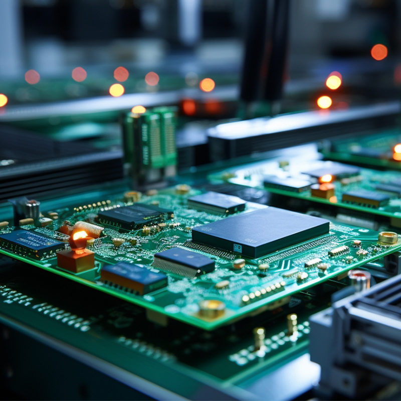
SCHEMATIC DESIGN of Blind-Buried Via PCB

This layout shows the exact appearance and placement of the components on Blind-Buried Via PCB.

