
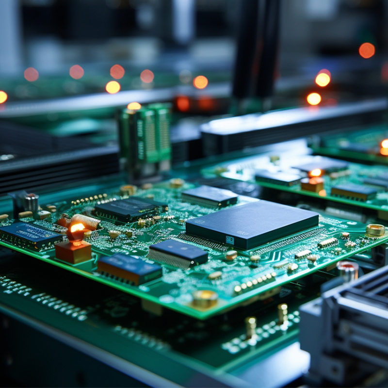
Buried Via PCB
Mintec Innovation Technology Industry Co., Ltd was established in 2004, with 20 years of experience in PCB manufacturing and PCBA assembly, and a professional technical team. PCB and PCBA quality is stable and reliable, with high yield and fast speed. It has sample and mass production workshops, and batch and sample have independent production lines.
The products are suitable for industries including: industrial,LED lighting,telecommunication,IOT, etc. Our factory has advanced equipment such as automatic graphics electroplating production lines,CNC drilling,flying probe tests and automatic test machines,laser exposure machines. And the products have obtained IC,C-Tick,CE,FCC and other certifications. The products are exported to Oceania,Europe,Africa,Asia , and other regions.

Buried Via PCB is one of our PCB products. We will introduce its detailed parameter information and our company advantages to you.
Tous nos produits sont strictement conformes aux réglementations RoHS/REACH, avec des prix abordables et une qualité inégalée. Le service OEM/ODM est disponible. Nous avons une grande expérience dans l'exportation et la gestion de projet, pour assurer votre commande 100%.
| Nom du produit | Buried Via PCB |
| Mot-clé | circuit card assembly,flexible pcb board,0.5 mm pcb,pcb assembly manufacturer |
| Lieu d'origine | Chine |
| Épaisseur du panneau | 1~3,2mm |
| Industries concernées | l'électronique grand public, etc. |
| Service | Fabrication OEM/ODM |
| Certificat | ISO-9001:2015, ISO-14001:2015,ISO-13485:2012.UL/CSA |
| Couleur du masque de soudure | Rouge |
| Avantage | Nous maintenons une bonne qualité et des prix compétitifs afin de garantir le bénéfice de nos clients. |
| Pays de vente | All over the world for example:Tokelau |
SCHEMATIC DESIGN of Buried Via PCB

Capacités de conception de MTI ID et MD

This layout shows the exact appearance and placement of the components on Buried Via PCB.

