Buried Via PCB
Mintec Innovation Technology Industry Co., Ltd was established in 2004, with 20 years of experience in PCB manufacturing and PCBA assembly, and a professional technical team. PCB and PCBA quality is stable and reliable, with high yield and fast speed. It has sample and mass production workshops, and batch and sample have independent production lines.
The products are suitable for industries including: industrial,LED lighting,telecommunication,IOT, etc. Our factory has advanced equipment such as automatic graphics electroplating production lines,CNC drilling,flying probe tests and automatic test machines,laser exposure machines. And the products have obtained IC,C-Tick,CE,FCC and other certifications. The products are exported to Oceania,Europe,Africa,Asia , and other regions.
Buried Via PCB is one of our PCB products. We will introduce its detailed parameter information and our company advantages to you.
All our products are strictly according to RoHS/REACH regulations, with affordable prices with unparalleled quality.We take care of our product quality, any defect of the goods, we will take responsibility. OEM/ODM service is available.We have full experience in exporting and project management, to secure your order 100%.
| Product name | Buried Via PCB |
| Keyword | circuit card assembly,flexible pcb board,0.5 mm pcb,pcb assembly manufacturer |
| Place of Origin | China |
| Board Thickness | 1~3.2mm |
| Applicable Industries | consumer electronics, etc. |
| Service | OEM/ODM manufacturing |
| Certificate | ISO-9001:2015, ISO-14001:2015,ISO-13485:2012.UL/CSA |
| Solder Mask Color | Red |
| Advantage | We keep good quality and competitive price to ensure our customers benefit |
| Sales country | All over the world for example:Tokelau |
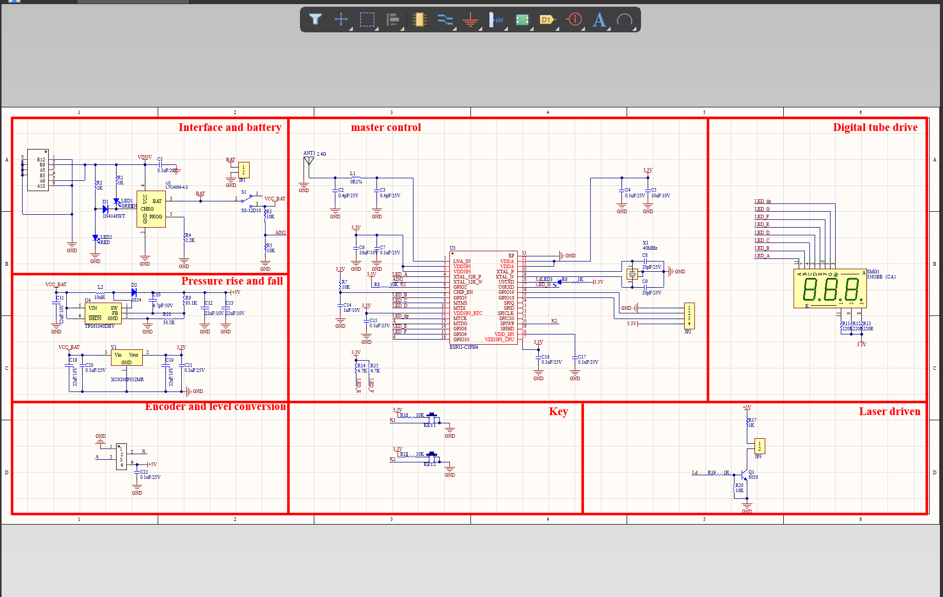
SCHEMATIC DESIGN of Buried Via PCB
MTI ID and MD Design Capabilities
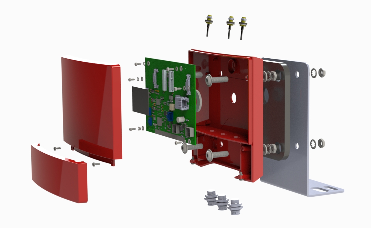
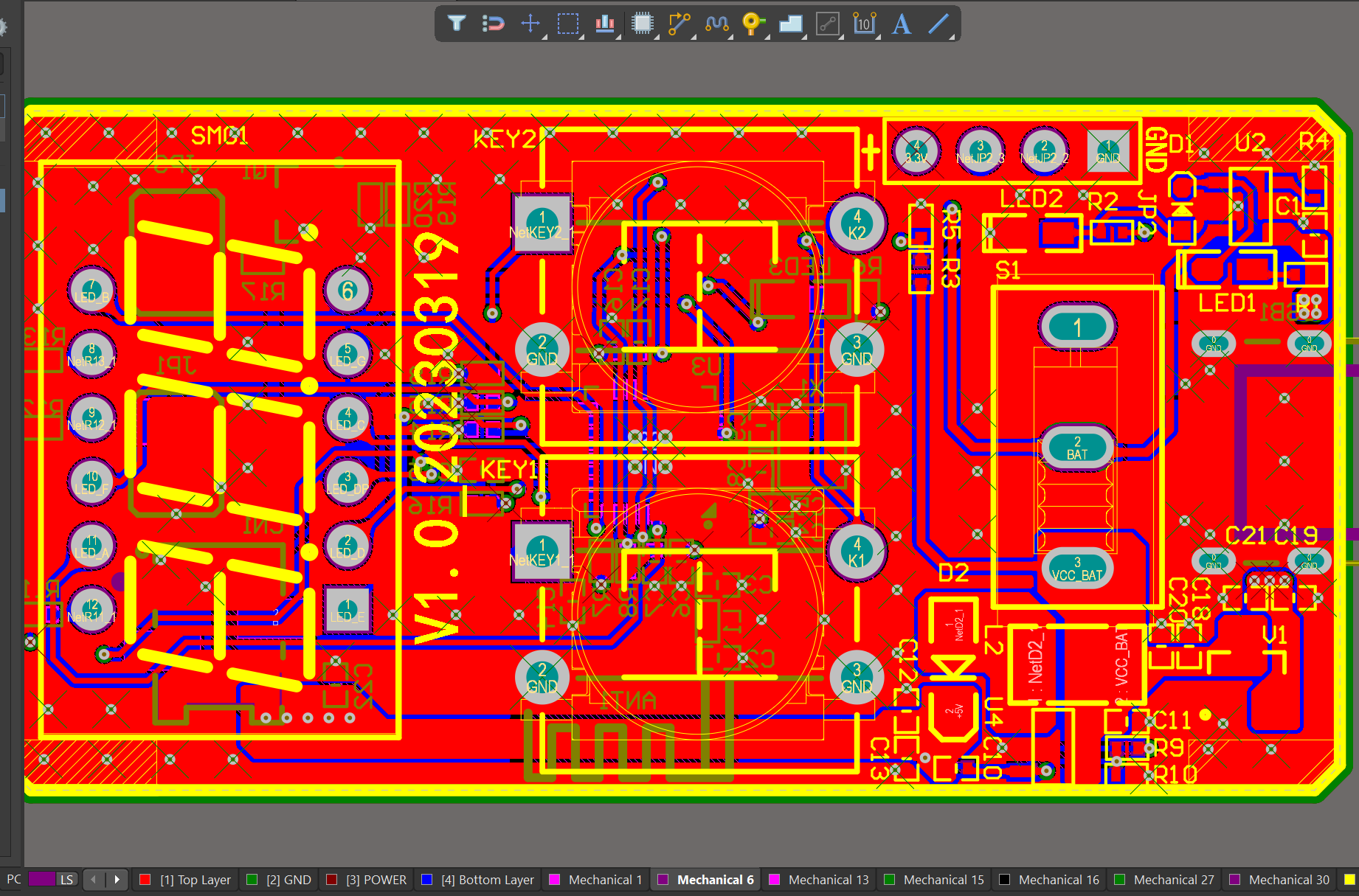
This layout shows the exact appearance and placement of the components on Buried Via PCB.
