Via cega PCB
Founded in 2004, Shenzhen Mintec Innovation Technology Industry is a high-tech enterprise with a plant area of5,000 square meters and more than 300 employees. It specializes in the production and sales of double-sided PCBs, multi-layer PCBs, high-resolution PCBs and high-quality PCBs. We have also introduced a full set of world-leading equipment, such as laser exposure machines,CNC drilling,graphics processing systems,milling machines, etc.
We focus on environmental management and quality system construction, and follow IPC-6012, IPC-TM-650, IPC-A-600G and PCB industry standards. We have successively obtained ISO9001, ISO14000, and ISO 13485 certifications. Our products are widely used in automotive industries,IOT,LED lighting,telecommunication and other industries. The classic marketing areas are in North America, Europe, China and Asia Pacific, and the products have been widely recognized by customers.

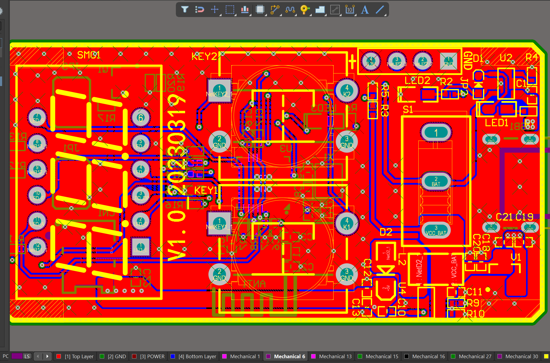
Blind Via PCB is one of our PCB products. We will introduce its detailed parameter information and our company advantages to you.
Todos os nossos produtos estão estritamente de acordo com as normas RoHS/REACH, com preços acessíveis e qualidade inigualável. Temos total experiência em exportação e gerenciamento de projetos, para garantir seu pedido 100%.
| Nome do produto | Via cega PCB |
| Palavra-chave | circuit card assembly,0.5 mm pcb,pcb manufacturer,pcb manufacturing,PCBA Assembly |
| Local de origem | China |
| Espessura da placa | 1~3,2 mm |
| Setores aplicáveis | nova energia, etc. |
| Serviço | Fabricação OEM/ODM |
| Certificado | ISO-9001:2015, ISO-14001:2015,ISO-13485:2012.UL/CSA |
| Cor da máscara de solda | Azul |
| Vantagens | Mantemos a boa qualidade e o preço competitivo para garantir que nossos clientes se beneficiem |
| País de vendas | All over the world for example:Christmas Island |
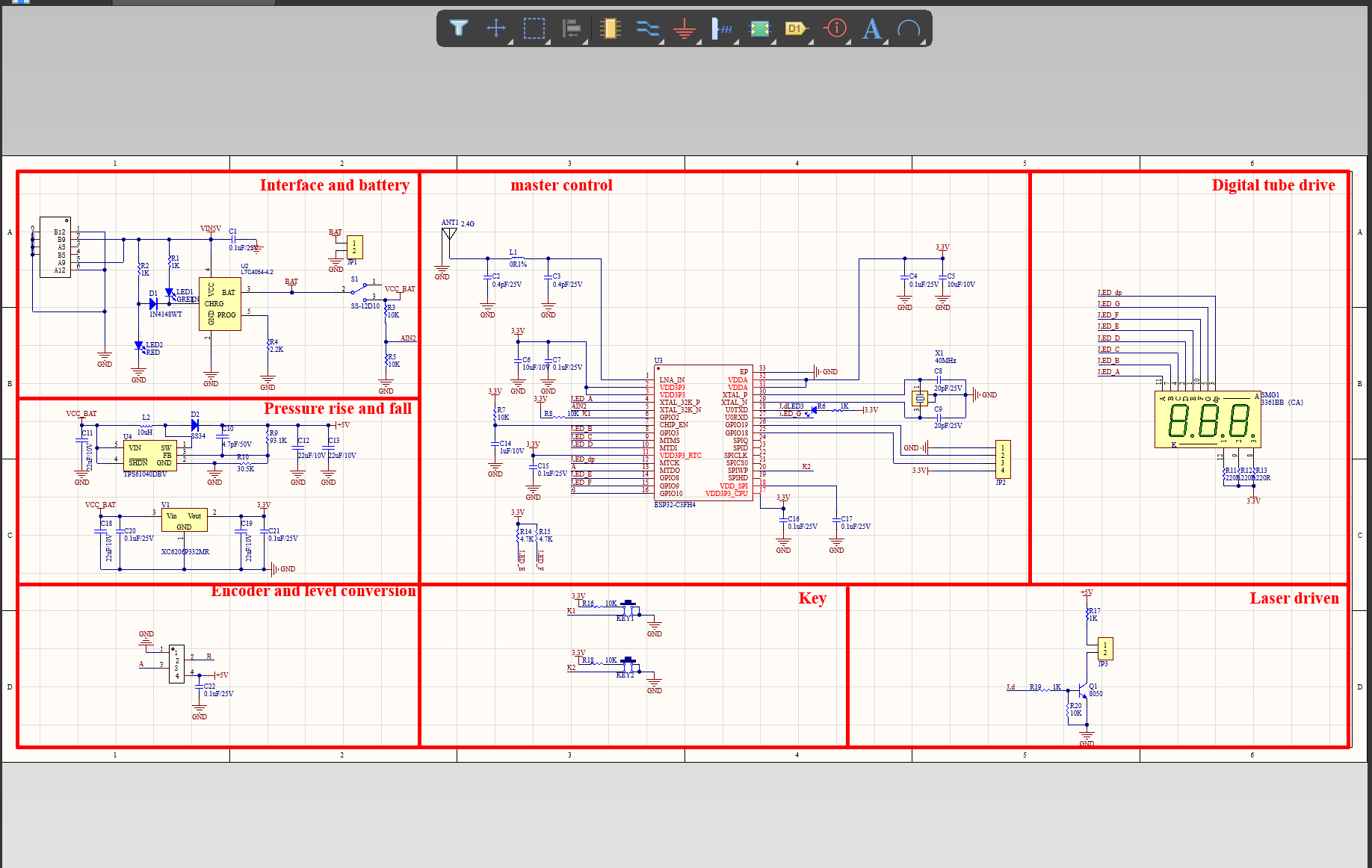
SCHEMATIC DESIGN of Blind Via PCB
Recursos de projeto de ID e MD da MTI
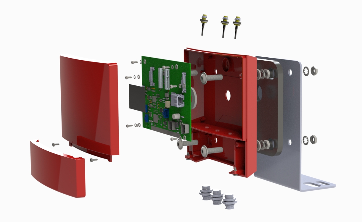
This layout shows the exact appearance and placement of the components on Blind Via PCB.
