
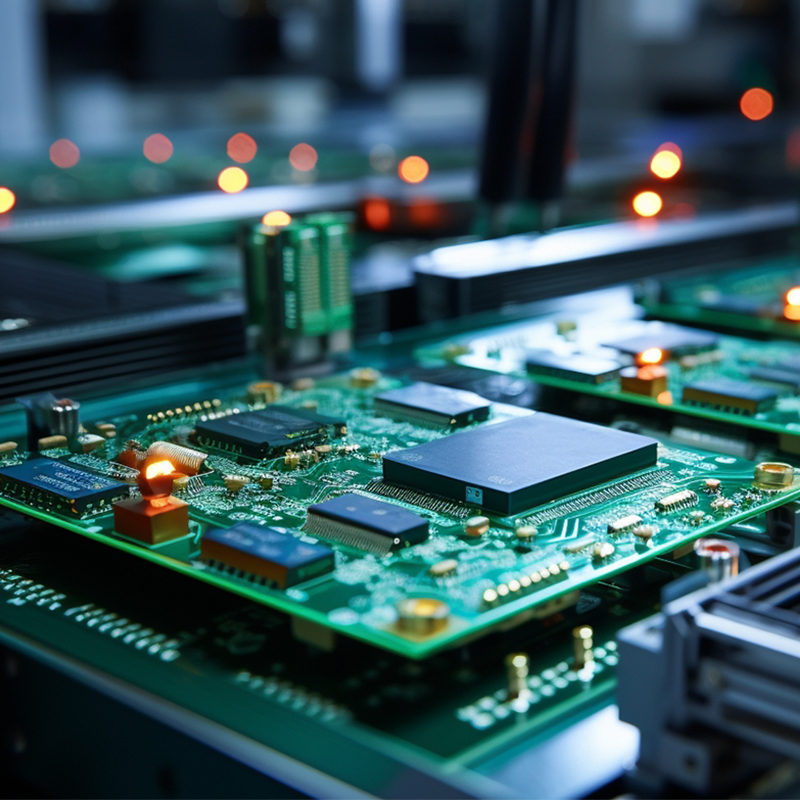
Buried Via PCB
Mintec Innovation Technology Industry Co., Ltd was established in 2004, with 20 years of experience in PCB manufacturing and PCBA assembly, and a professional technical team. PCB and PCBA quality is stable and reliable, with high yield and fast speed. It has sample and mass production workshops, and batch and sample have independent production lines.
The products are suitable for industries including: industrial,LED lighting,telecommunication,IOT, etc. Our factory has advanced equipment such as automatic graphics electroplating production lines,CNC drilling,flying probe tests and automatic test machines,laser exposure machines. And the products have obtained IC,C-Tick,CE,FCC and other certifications. The products are exported to Oceania,Europe,Africa,Asia , and other regions.

Buried Via PCB is one of our PCB products. We will introduce its detailed parameter information and our company advantages to you.
Alle unsere Produkte sind streng nach RoHS/REACH-Vorschriften, mit erschwinglichen Preisen mit unvergleichlicher Qualität.Wir kümmern uns um unsere Produktqualität, jeder Fehler der Ware, werden wir die Verantwortung übernehmen. Wir haben volle Erfahrung im Export und Projektmanagement, um Ihre Bestellung 100% zu sichern.
| Name des Produkts | Buried Via PCB |
| Schlüsselwort | circuit card assembly,flexible pcb board,0.5 mm pcb,pcb assembly manufacturer |
| Ort der Herkunft | China |
| Dicke der Platte | 1~3,2mm |
| Anwendbare Industrien | Unterhaltungselektronik, usw. |
| Dienst | OEM/ODM-Fertigung |
| Zertifikat | ISO-9001:2015, ISO-14001:2015,ISO-13485:2012.UL/CSA |
| Farbe der Lötmaske | Rot |
| Vorteil | Wir sorgen für gute Qualität und wettbewerbsfähige Preise, damit unsere Kunden davon profitieren. |
| Verkaufsland | All over the world for example:Tokelau |
SCHEMATIC DESIGN of Buried Via PCB

MTI ID und MD Design-Fähigkeiten

This layout shows the exact appearance and placement of the components on Buried Via PCB.

