Quais são os diferentes tipos de placas de circuitos impressos e as suas utilizações?

Printed circuit boards (PCB) are essential components found in almost all electronic devices. They are the backbone of modern technology, providing a means to connect and organize electronic components, allowing them to function smoothly. There are various types of printed circuit boards, each with its unique design and purpose. In this article, we will explore the different types of PCB and their uses.

Single-sided PCB:

A single-sided PCB is the most basic type of circuit board and is the most commonly used. As the name suggests, this type of board only has one layer of conductive material (usually copper) on one side. Passive components such as resistors, capacitors, and diodes are placed on the top side of the board, while all the traces (electrical pathways) and solder pads are on the bottom side. The use of single-sided PCB is typically limited to simple, low-cost devices such as calculators, toys, and LED lights.

Double-sided PCB:

A double-sided PCB has conductive material on both sides of the board, allowing for more complex circuit designs. This type of board is commonly used for more advanced electronic devices, such as printers, mobile phones, and home appliances. The components are mounted on both sides of the board, and the traces are routed through vias (small holes drilled in the board) to connect the top and bottom layers. Double-sided PCB are relatively affordable and more versatile than single-sided ones.

Multi-layer PCB:

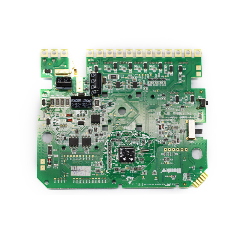
As the name implies, a multi-layer PCB has multiple layers of conductive material and insulating material, sandwiched together to form a single board. This type of board is typically used for advanced electronic devices, where space is limited, and high functionality is required. Multi-layer PCB are commonly used in computers, routers, and other complex devices. They can have anywhere from 4 to 20+ layers, depending on the complexity of the circuit layout.

Rigid PCB:

A rigid PCB is the most common type of PCB and is made of rigid materials such as fiberglass or epoxy resin. It is stiff and cannot be bent, making it suitable for most electronic devices. Rigid PCB are available in single, double, and multi-layer configurations.

Flexible PCB:

A flexible PCB, also known as a flex PCB, is made of flexible materials such as polyimide or polyester. These materials allow the board to bend or twist, making them ideal for electronic devices that require a custom shape. Flex PCB are commonly used in consumer electronics, such as smartphones, tablets, and wearables. They are also used in aerospace, military, and medical applications, where weight, size, and durability are crucial factors.

Rigid-Flex PCB:

A rigid-flex PCB is a combination of rigid and flexible PCB, providing both advantages within a single board. This type of board is designed to have a rigid section for components that require stability and a flexible section for moving or bending parts. These boards are commonly used in smartphones, cameras, and other electronic devices with moving parts.

High-Frequency PCB:

High-frequency PCB are designed to handle signals in the high-frequency range, typically above 1GHz. They are made of special materials, such as PTFE (polytetrafluoroethylene) or ceramic, which have low dielectric loss and can maintain a stable signal. High-frequency PCB are used in applications such as satellite communications, radar systems, and medical equipment.

Metal-Core PCB:

A metal-core PCB has a metal layer as the base, usually aluminum, with a layer of insulating material on top and a layer of copper on the bottom. This type of board is commonly used for high-power applications, as the metal layer acts as a heat sink, dissipating heat generated by the components. Metal-core PCB are used in LED lighting, power supplies, and automotive electronics.

High-Density Interconnect (HDI) PCB:

HDI PCB are designed to have a high-density of components in a compact space. They use microvias, blind vias, and buried vias to connect the layers, allowing for a more complex and compact circuit design. HDI PCB are used in smartphones, tablets, laptops, and other compact electronic devices.

Integrated Circuit (IC) Substrate PCB:

IC substrate PCB are used to mount the integrated circuits (ICs) of electronic devices. They are typically made of ceramic or glass material, and the ICs are mounted on top using wire bonding or flip-chip technology. IC substrate PCB are used in computers, telecommunications, and other electronic devices that require advanced microchips.

In conclusion, printed circuit boards come in various shapes, sizes, and configurations to suit different electronic devices. Each type of PCB has its unique design and purpose, making them essential components of modern technology. As technology continues to evolve, so will the design and use of printed circuit boards, making them an integral part of our daily lives.

Introdução às placas de circuitos impressos: Entendendo o básico

Printed Circuit Boards (PCB) are widely used in today’s electronic devices, such as smartphones, computers, and even household appliances. They are an essential component in the manufacturing of electronic products and have greatly evolved over the years. In this article, we will delve into the basics of PCB – how they work, their types, and their key components.

What is a Printed Circuit Board?

A Printed Circuit Board, also known as a PCB, is a thin board made of non-conductive material, usually fiberglass, that serves as the base for mounting and connecting electronic components. It is designed to provide a stable platform for the attachment of electrical components and serves as an interconnected pathway for the flow of electric signals between them. The board is printed with thin layers of conductive material, typically copper, which forms the circuitry and allows for the transmission of electricity.

Types of Printed Circuit Boards

There are various types of PCB  each serving a different purpose. The most commonly used types are single-sided, double-sided, and multi-layer PCBs.

1. Single-Sided PCB: These are the most basic and commonly used type of PCB. They have a layer of conductive material, usually copper, on one side of the board, and the components are mounted on the other side. Single-sided PCB are mainly used in simple electronics with relatively few components.

2. Double-Sided PCB: As the name suggests, double-sided PCB have a layer of conductive material on both sides of the board. This allows for greater flexibility in design and enables the use of more complex circuits.

3. Multi-Layer PCB: These PCBs consist of several layers of conductive material separated by insulating layers, with the components mounted on the outer layers. Multi-layer PCB are used in complex electronics where space is limited and compact designs are required.

Key Components of a Printed Circuit Board

1. Substrate: The substrate is the base material of the PCB, usually made of fiberglass or composite epoxy material. It provides the necessary support for the conductive layers and components.

2. Conductive Layers: These are thin layers of conductive material, typically copper, that make up the circuitry of the PCB. They are usually etched onto the substrate and are responsible for carrying the electrical signals between components.

3. Components: Electronic components such as resistors, capacitors, and integrated circuits (ICs) are mounted on the PCB. They are connected to the conductive layers through holes called vias or by traces on the surface of the board.

4. Solder Mask: The solder mask is a protective layer that covers the conductive layers, leaving only the connection points exposed. It protects the PCB from corrosion and protects against short circuits.

5. Silkscreen: This is the layer on top of the solder mask that is used to label and identify components and their placement on the board. It usually contains information such as component names, reference numbers, and polarity.

How do Printed Circuit Boards Work?

The functioning of a PCB is relatively simple. The components on the board are connected by a network of conductive paths, also known as traces, which allow the flow of electricity between them. These paths are created by etching the conductive layers, usually copper, to form a pattern that connects the components in the desired configuration.

The components are mounted on the board by soldering them to the conductive pads, which serve as connection points. The soldering process involves heating the pads and components, then melting the soldering material, usually a mixture of tin and lead, to create a strong and permanent bond.

Advantages of Using Printed Circuit Boards

The use of PCBs offers several advantages over other methods of connecting electronic components. These include:

1. Compact and Lightweight: PCBs are compact and lightweight, making them ideal for use in smaller electronic devices.

2. High Reliability: Due to their design and manufacturing process, PCBs have proven to be highly reliable and durable.

3. Cost-effective: The use of PCBs significantly reduces the cost of production and assembly of electronic devices, making them a cost-effective option.

4. Easy to Repair and Replace: In the event of a faulty component, the PCB can be easily repaired or replaced without the need for complex and time-consuming re-wiring.

Conclusão

Printed Circuit Boards are vital components in today’s electronic devices, allowing for compact and efficient designs. They come in various types, each serving different purposes, and are made up of key components such as the substrate, conductive layers, components, solder mask, and silkscreen. Their use offers numerous advantages, making them an essential element in the manufacturing of electronic products. As technology continues to advance, we can expect to see further advancements in the design and use of PCBs.


The Evolution of Printed Circuit Boards: From Early Designs to Modern Technology

Printed circuit boards (PCBs) are an essential component in most modern electronic devices. They serve as the foundation for electronic connections and are responsible for routing the electrical signals between the different components of a circuit. PCBs have undergone significant changes since their first inception, and their evolution has closely mirrored advancements in technology.

The Early Days

The origin of PCBs can be traced back to the late 19th century when they were used in a rudimentary form for telephone exchanges. These early PCBs were known as “printed wires” and were created by attaching thin metal wires to a wooden board. This early form of PCB was used to connect telephone switchboards and reduce the need for manual rewiring.

In the early 1900s, scientists started experimenting with the use of thin copper foils on flat bases to create electrical circuits. This led to the invention of “printed” wires on flat boards made by hand, which also reduced the size and complexity of electronic devices. These early PCBs were primarily used in military equipment and radios during World War II.

The Advent of Mass Production

The first commercially successful mass-produced PCB was developed in 1942 by Paul Eisler, an Austrian inventor. His innovative design used conductive ink on a Bakelite board, marking the beginning of modern PCB technology. His creation was initially used in the radio industry, but its use quickly spread to other electronic devices.

The introduction of transistors in the 1950s revolutionized the electronic industry. This development led to smaller and more efficient devices, and PCBs played a crucial role in their production. The early PCB designs used point-to-point connections, which limited the complexity and size of circuits. However, with the introduction of transistors, manufacturers were able to add more components to a PCB, leading to the creation of more advanced electronic devices.

The Rise of Integrated Circuits

In the late 1950s, scientists developed the first integrated circuit (IC), which was a significant breakthrough in the evolution of PCBs. ICs allowed for the miniaturization of electronic components, making devices smaller, faster, and more efficient. This technology paved the way for PCBs to become an integral part of electronic devices, from televisions and radios to computers and mobile phones.

As electronic devices became more complex and the demand for smaller and more efficient devices increased, PCBs continued to evolve. In the 1960s, the through-hole method of assembling components on a PCB was introduced, which allowed for the use of larger and more complex circuits. This method involved drilling holes into the board and inserting component wires through them before soldering them in place.

The Rise of Surface Mount Technology (SMT)

In the 1980s, surface mount technology (SMT) was introduced, bringing another significant change to the manufacturing of PCBs. SMT involves attaching components directly onto the surface of a PCB, eliminating the need for drilling holes. This method increased the complexity and density of electronic circuits, making devices even smaller and more powerful.

SMT also allowed for the use of automated assembly processes, reducing the cost and time required to produce PCBs. This resulted in the mass production of electronic devices, making them more accessible and affordable for the general population.

The Evolution Continues

The evolution of PCBs is ongoing, with new advancements and innovations being introduced regularly. Today, manufacturers are using advanced techniques, such as multi-layer PCBs and flexible PCBs, to further improve the performance and capabilities of electronic devices.

Multi-layer PCBs have multiple layers of circuitry, allowing for more complex circuits without increasing the size of the board. This technology is used in devices such as computers and smartphones, where space is limited, but functionality is crucial.

Flexible PCBs, as the name suggests, can be bent or twisted without damaging the circuitry. This technology has allowed for the creation of devices such as foldable smartphones and wearable technology, where rigid PCBs would not be suitable.

In addition to these advancements, there has also been a push towards more environmentally friendly PCB production. Lead-free and halogen-free materials are being used, and recycling methods are being developed to reduce the impact of electronic waste on the environment.

Understanding the specific demands concerning varistors in Montagem de PCB (PCBA) design is essential. Here’s a breakdown of what PCBA design demands from varistors:

Operating Temperature/Storage:

Maintain the working temperature of the circuit within the specified range outlined in the product’s specifications. After montagem, store the circuit within the product’s specified temperature range when it’s not operational. Avoid using temperatures higher than the specified maximum operating temperature.

Operating Voltage:

Keep the voltage applied across the varistor terminals below the maximum permissible voltage. Incorrect usage might result in product failure, short circuits, or potential heating issues. Although the usage voltage should be below the rated voltage, in cases of continuous high-frequency or pulse voltage, thoroughly assess the varistor’s reliability.

Component Heating:

Ensure that the surface temperature of the varistor remains below the highest specified operating temperature (considering temperature elevation caused by the component’s self-heating) as dictated in the product specifications. Confirm varistor temperature elevation due to circuit conditions under the actual operational state of the equipment.

Restricted Usage Areas:

  • Varistors shouldn’t be used in the following environments:
  • Places with water or saltwater.
  • Areas prone to condensation.
  • Locations with corrosive gases (such as hydrogen sulfide, sulfur dioxide, ammonia, etc.).
  • Conditions where the vibration or shock exceeds the specified range in the product specifications.

PCB Selection:

The performance of aluminum oxide circuit boards may deteriorate due to thermal shock (temperature cycling). It’s crucial to confirm if the circuit board affects the product quality during use.

Pad Size Setting:

More soldering leads to increased pressure on the varistor, leading to quality issues like surface cracks. Therefore, when designing the solder pad on the circuit board, suitable shapes and sizes must be set according to the soldering volume. Maintain an equal size for the solder pads. Uneven solder volumes on the left and right pads can cause delayed solidification on the side with more solder, leading to stress-induced cracks on the other side during solder cooling.

Component Configuration:

Installing varistors in PCBA or subjecting circuit boards to bending during operation may result in varistor fractures. Hence, configuring components must consider the circuit board’s resistance to bending and avoid applying excessive pressure.

No processo de produção diário, a atenção meticulosa a vários pormenores de produção é crucial para garantir uma qualidade de fabrico superior. Cumprir rigorosamente os requisitos estipulados com uma abordagem dedicada e responsável durante a produção é fundamental para um processamento optimizado, que é essencial para a manutenção do crescimento da empresa. Abaixo, a nossa equipa da fábrica de montagem SMT em MTI PCBA compilou um guia para as principais considerações durante os processos de montagem SMT. Vamos aprofundá-lo em conjunto:

Temperatura e humidade da oficina

Manter as condições ideais na oficina de produção é essencial. Para as oficinas SMT, a temperatura ideal é de 24±2℃, com níveis de humidade à volta de 40±10%RH. Temperaturas extremas podem levar a problemas de solda, como contas de estanho ou bolhas de solda e problemas relacionados ao estêncil durante a impressão.

Armazenamento de materiais

Na montagem pré-SMT, as condições de armazenamento dos materiais são frequentemente ignoradas. Por exemplo, as placas de circuito impresso expostas ao ar durante longos períodos tendem a absorver humidade, o que resulta numa soldadura deficiente mais tarde. Além disso, é necessária uma atenção especial para o armazenamento de chips BGA e IC, que requerem um ambiente seco para evitar a oxidação.

Pasta de solda

A pasta de solda, um material essencial na montagem SMT, é composta principalmente por pó de estanho e fluxo. Uma vez que o fluxo desempenha um papel significativo em todo o processo de soldadura, é crucial selecionar uma pasta de solda de alta qualidade. Os procedimentos de pré-utilização, como o refluxo e a agitação da pasta de solda, são pormenores essenciais a não descurar.

Processo de soldadura

O processo de soldadura por refluxo ocupa uma posição crítica na montagem SMT, tendo um impacto direto na qualidade da soldadura. A qualidade da soldadura de montagem em superfície é um dos factores mais críticos. As considerações sobre a soldadura por refluxo envolvem normalmente a temperatura do forno, o pré-aquecimento e as temperaturas óptimas.

Controlo de qualidade pós-refluxo (QC)

A qualidade do produto representa a reputação da fábrica, e a qualidade da soldadura influencia-a significativamente. Produtos excepcionais são essenciais para manter uma vantagem competitiva no mercado. PCBA indústria. Assim, é imperativo um controlo rigoroso da qualidade do processo de soldadura, concentrando-se nos pormenores para evitar defeitos como juntas de soldadura abertas, saltos de soldadura ou pontes.

Para mais informações sobre prototipagem rápida na montagem SMT, high-end PCBA fabrico, SMT preços de montagem e muito mais, sinta-se à vontade para explorar MTI PCBA  para obter informações pormenorizadas.

Capacitando a conetividade: A evolução da tecnologia 5G CPE

O 5G CPE, ou 5G Customer Premise Equipment, é um dispositivo que se liga a uma rede 5G e fornece acesso à Internet a outros dispositivos através de Wi-Fi ou Ethernet. O CPE 5G pode oferecer um serviço de Internet mais rápido e fiável do que os routers ou modems tradicionais, uma vez que pode suportar uma maior largura de banda, menor latência e uma cobertura mais ampla. Neste artigo, partilharemos a nossa experiência de desenvolvimento de CPE 5G, desde a conceção esquemática à montagem de PCB.

Desenho esquemático

O primeiro passo do nosso processo de desenvolvimento foi desenhar o esquema do dispositivo CPE 5G. O esquema é uma representação gráfica das ligações eléctricas e dos componentes do dispositivo. O esquema mostra como a fonte de alimentação, o módulo 5G, o módulo Wi-Fi, o módulo Ethernet, a antena e outros componentes estão ligados e configurados. O esquema também especifica os valores e as classificações das resistências, condensadores, indutores, díodos, transístores e outros componentes.

Para desenhar o esquema, utilizámos o [EAGLE], uma ferramenta de software que nos permite criar e editar diagramas esquemáticos de forma fácil e eficiente. O EAGLE tem uma biblioteca de milhares de componentes normalizados que podemos arrastar e largar no nosso esquema. O EAGLE também tem uma funcionalidade de simulação que nos permite testar e verificar o nosso esquema antes de avançarmos para o passo seguinte.

Disposição da placa de circuito impresso

O segundo passo do nosso processo de desenvolvimento foi conceber a disposição da placa de circuito impresso do dispositivo CPE 5G. A disposição da placa de circuito impresso é uma representação física da disposição e colocação dos componentes e dos traços na placa de circuito impresso. O layout da PCB mostra como os componentes são montados na placa, como os traços são roteados entre eles e como a placa é moldada e dimensionada.

Para conceber a disposição da placa de circuito impresso, utilizámos o [KiCad], uma ferramenta de software que nos permite criar e editar disposições de placas de circuito impresso de forma fácil e eficiente. O KiCad tem uma funcionalidade que nos permite importar o nosso esquema do EAGLE e gerar automaticamente um esquema de PCB com base no mesmo. O KiCad também tem um visualizador 3D que nos permite ver como é que o nosso esquema de PCB se parece na vida real.

Montagem de PCB

O terceiro e último passo do nosso processo de desenvolvimento foi a montagem da placa de circuito impresso do dispositivo CPE 5G. A montagem da PCB é o processo de soldar os componentes na placa de circuito impresso de acordo com o esquema da PCB. A montagem da placa de circuito impresso requer precisão e rigor, uma vez que qualquer erro ou defeito pode afetar o desempenho ou a funcionalidade do dispositivo.

Para montar a placa de circuito impresso, utilizámos a [JLCPCB], um fabricante profissional de placas de circuito impresso que oferece serviços de montagem de placas de circuito impresso de alta qualidade a preços baixos. A JLCPCB tem uma funcionalidade que nos permite carregar o nosso ficheiro de esquema de PCB e encomendar as nossas PCBs online. JLCPCB também tem um grande inventário de componentes padrão que podemos escolher para a nossa montagem de PCB. A JLCPCB pode entregar as nossas placas de circuito impresso montadas em poucos dias.

Desenvolvemos com êxito o CPE 5G, desde a conceção esquemática até à montagem da placa de circuito impresso, utilizando várias ferramentas e serviços de software. Aprendemos muito com este projeto e estamos orgulhosos do nosso feito. Esperamos que a nossa experiência de desenvolvimento possa inspirar e ajudar outras pessoas interessadas em criar os seus próprios dispositivos 5G CPE. Se tiver alguma questão ou comentário, não hesite em contactar-nos. Obrigado pela leitura.


Chicote de fios vs. Conjunto de cabos: Compreender as diferenças

O que é um chicote de fios?

Um cablagem é um conjunto de fios ou cabos que são enrolados ou unidos por um material externo, como PVC, borracha ou nylon. O objetivo de um cablagem é manter os fios ou cabos limpos e arrumados e facilitar a sua instalação e manutenção. Um cablagem não oferece grande proteção aos fios ou cabos no seu interior, uma vez que estes já estão normalmente isolados pelas suas próprias bainhas. Um cablagem é utilizada principalmente para organizar os fios ou cabos que se encontram num ambiente relativamente seguro e estável, como o interior de uma caixa de computador, o painel de instrumentos de um automóvel ou um eletrodoméstico.


Vantagens dos cablagens

  • Fiabilidade: Os chicotes de fios asseguram ligações eléctricas consistentes e fiáveis, reduzindo o risco de curto-circuitos ou ligações soltas.
  • Instalação simplificada: Simplificam os processos de instalação, eliminando a necessidade de ligar os fios individuais um a um.
  • Manutenção melhorada: A etiquetagem e a organização facilitam a identificação e a substituição de componentes defeituosos quando necessário.
  • Eficiência de espaço: Os cablagens ajudam a gerir e a otimizar a utilização do espaço nos dispositivos e sistemas electrónicos.

O que é um conjunto de cabos?

Um conjunto de cabos é um grupo de fios ou cabos que são envolvidos por uma única cobertura de proteção, como termoplástico, vinil ou metal. O objetivo de um conjunto de cabos é proteger os fios ou cabos de factores externos, como o calor, a humidade, a abrasão, a vibração, os produtos químicos ou as interferências electromagnéticas. Um conjunto de cabos foi concebido para resistir a condições difíceis e exigentes, como em maquinaria industrial, equipamento exterior ou aplicações aeroespaciais

As cablagens e os conjuntos de cabos são duas soluções diferentes para organizar e proteger os componentes eléctricos. As cablagens são feixes de fios ou cabos de baixo custo e fáceis de instalar que são envolvidos ou unidos por um material externo. Os conjuntos de cabos são grupos de fios ou cabos de alta proteção e alto desempenho que são envolvidos por uma única cobertura de proteção. A escolha entre cablagens e conjuntos de cabos depende do ambiente, do desempenho, do espaço e do orçamento da aplicação. Para mais informações sobre cablagens e conjuntos de cabos, contacte MTI agora !


Lorem Ipsum é simplesmente o texto fictício da indústria gráfica e tipográfica. O Lorem Ipsum tem sido o texto fictício padrão da indústria desde os anos 1500