
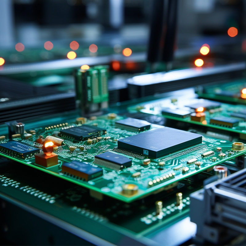
Buried Via PCB
Mintec Innovation Technology Industry Co., Ltd was established in 2004, with 20 years of experience in PCB manufacturing and PCBA assembly, and a professional technical team. PCB and PCBA quality is stable and reliable, with high yield and fast speed. It has sample and mass production workshops, and batch and sample have independent production lines.
The products are suitable for industries including: industrial,LED lighting,telecommunication,IOT, etc. Our factory has advanced equipment such as automatic graphics electroplating production lines,CNC drilling,flying probe tests and automatic test machines,laser exposure machines. And the products have obtained IC,C-Tick,CE,FCC and other certifications. The products are exported to Oceania,Europe,Africa,Asia , and other regions.

Buried Via PCB is one of our PCB products. We will introduce its detailed parameter information and our company advantages to you.
Tutti i nostri prodotti sono rigorosamente conformi alle normative RoHS/REACH, con prezzi accessibili con qualità ineguagliabile.Ci prendiamo cura della nostra qualità del prodotto, qualsiasi difetto delle merci, ci assumeremo la responsabilità. Servizio OEM/ODM è disponibile.Abbiamo piena esperienza nell'esportazione e nella gestione del progetto, per garantire il vostro ordine 100%.
| Nome del prodotto | Buried Via PCB |
| Parola chiave | circuit card assembly,flexible pcb board,0.5 mm pcb,pcb assembly manufacturer |
| Luogo di origine | Cina |
| Spessore del pannello | 1~3,2 mm |
| Industrie applicabili | elettronica di consumo, ecc. |
| Servizio | Produzione OEM/ODM |
| Certificato | ISO-9001:2015, ISO-14001:2015,ISO-13485:2012.UL/CSA |
| Colore della maschera di saldatura | Rosso |
| Vantaggio | Manteniamo una buona qualità e un prezzo competitivo per garantire ai nostri clienti di trarne vantaggio. |
| Paese di vendita | All over the world for example:Tokelau |
SCHEMATIC DESIGN of Buried Via PCB

Capacità di progettazione MTI ID e MD

This layout shows the exact appearance and placement of the components on Buried Via PCB.

