
2.4 ghz yagi pcb antenna
MTI is a professional manufacturer of PCB and PCBA , we supply one-stop service. The company’s main services include PCB production, PCB Assembly and electronic materials purchasing, SMT patch, circuit board welding, circuit board plug-in.
Our clientele spans across major continents (Africa,America,Oceania)and encompasses various industries, including healthcare,industrial control
| Product name | 2.4 ghz yagi pcb antenna |
| Keyword | 120mm pcb,12v pcb |
| Place of Origin | China |
| Board Thickness | 2~3.2mm |
| Applicable Industries | medical, etc. |
| Service | OEM/ODM manufacturing |
| Certificate | ISO-9001:2015, ISO-14001:2015,ISO-13485:2012.UL/CSA |
| Solder Mask Color | Red |
| Advantage | We keep good quality and competitive price to ensure our customers benefit |
| Sales country | All over the world for example:Kyrgyzstan,Holy See (Vatican City),Monaco,Malaysia,Romania |
We have rich experience engineer to create a layout using a software platform like Altium Designer. This layout shows you the exact appearance and placement of the components on your board.

One of our Hardware Design Services is small-batch manufacturing, which allows you to test your idea quickly and verify the functionality of the hardware design and PCB board,2.4 ghz yagi pcb antenna.

Your deliverables are always ahead of schedule and of the highest quality.

FAQs Guide
2.How do PCBs handle overcurrent and short circuits?
3.Can PCBs be designed to withstand high vibration or shock?
4.Can PCBs be customized based on specific design requirements?
5.How does component placement affect signal integrity in a PCB design?
6.What are the key features of a PCB?
1.How do PCBs support the integration of different electronic components?
We actively participate in the 2.4 ghz yagi pcb antenna industry associations and organization activities. The corporate social responsibility performed well, and the focus of brand building and promotion.
PCBs (Printed Circuit Boards) are essential for the integration of different electronic components in electronic devices. They provide a platform for connecting and supporting the various components, allowing them to work together seamlessly. Here are some ways in which PCBs support the integration of different electronic components:
1. Electrical connections: PCBs have a network of copper traces that connect the different electronic components on the board. These traces act as conductors, allowing electricity to flow between the components and enabling them to communicate and work together.
2. Mounting surface: PCBs provide a stable and secure mounting surface for electronic components. The components are soldered onto the board, ensuring that they are firmly attached and will not move or become loose during operation.
3. Space-saving: PCBs are designed to be compact and space-saving, allowing for the integration of multiple components on a single board. This is especially useful in small electronic devices where space is limited.
4. Customization: PCBs can be customized to accommodate different types and sizes of electronic components. This allows for flexibility in design and the integration of a wide range of components, making it easier to create complex electronic devices.
5. Signal routing: PCBs have multiple layers, with each layer dedicated to a specific function. This allows for efficient routing of signals between components, reducing interference and ensuring that the components can communicate effectively.
6. Power distribution: PCBs have dedicated power planes that distribute power to the different components on the board. This ensures that each component receives the required amount of power, preventing damage and ensuring proper functioning.
7. Thermal management: PCBs also play a crucial role in managing the heat generated by electronic components. They have copper layers that act as heat sinks, dissipating heat and preventing the components from overheating.
In summary, PCBs provide a robust and efficient platform for integrating different electronic components. They enable the components to work together seamlessly, ensuring the proper functioning of electronic devices.
2.How do PCBs handle overcurrent and short circuits?
We have a first -class management team, and we pay attention to teamwork to achieve common goals.
PCBs (printed circuit boards) have several mechanisms in place to handle overcurrent and short circuits:
1. Fuses: Fuses are the most common protection mechanism used on PCBs. They are designed to break the circuit when the current exceeds a certain threshold, preventing damage to the components and the board.
2. Circuit breakers: Similar to fuses, circuit breakers are designed to break the circuit when the current exceeds a certain threshold. However, unlike fuses, circuit breakers can be reset and reused.
3. Overcurrent protection devices: These devices, such as overcurrent protection diodes, are designed to limit the amount of current flowing through the circuit. They act as a safety valve, preventing excessive current from damaging the components.
4. Thermal protection: Some PCBs have thermal protection mechanisms, such as thermal fuses or thermal cutoffs, which are designed to break the circuit when the temperature of the board exceeds a certain threshold. This helps prevent damage to the board and components due to overheating.
5. Short circuit protection: PCBs may also have short circuit protection mechanisms, such as polymeric positive temperature coefficient (PPTC) devices, which are designed to limit the current in the event of a short circuit. These devices have a high resistance at normal operating temperatures, but their resistance increases significantly when the temperature rises due to a short circuit, limiting the current flow.
Overall, PCBs use a combination of these protection mechanisms to handle overcurrent and short circuits, ensuring the safety and reliability of the board and its components.

3.Can PCBs be designed to withstand high vibration or shock?
We have established long-term and stable partnerships with our suppliers, so we have great advantages in price and cost and quality assurance.
Yes, PCBs can be designed to withstand high vibration or shock by incorporating certain design features and using appropriate materials. Some ways to make a PCB more resistant to vibration and shock include:
1. Using a thicker and more rigid PCB substrate material, such as FR-4 or ceramic, to provide better structural support and reduce flexing.
2. Adding additional support structures, such as mounting holes or stiffeners, to secure the PCB to the chassis or enclosure.
3. Using smaller and more compact components to reduce the overall weight and size of the PCB, which can help minimize the effects of vibration.
4. Using shock-absorbing materials, such as rubber or foam, between the PCB and the mounting surface to absorb and dampen vibrations.
5. Designing the PCB layout to minimize the length and number of traces and vias, which can reduce the risk of mechanical stress and failure.
6. Using surface mount technology (SMT) components instead of through-hole components, as they are less prone to damage from vibration.
7. Incorporating conformal coating or potting materials to protect the PCB and components from moisture and mechanical stress.
It is important to consider the specific requirements and environment in which the PCB will be used when designing for high vibration or shock resistance. Consulting with a PCB design expert can also help ensure that the PCB is properly designed to withstand these conditions.
4.Can PCBs be customized based on specific design requirements?
We have rich industry experience and professional knowledge, and have strong competitiveness in the market.
Yes, PCBs (printed circuit boards) can be customized based on specific design requirements. This is typically done through the use of computer-aided design (CAD) software, which allows for the creation of a custom layout and design for the 2.4 ghz yagi pcb antenna. The design can be tailored to meet specific size, shape, and functionality requirements, as well as incorporate specific components and features. The customization process may also involve selecting the appropriate materials and manufacturing techniques to ensure the PCB meets the desired specifications.

5.How does component placement affect signal integrity in a PCB design?
We pay attention to the transformation of intellectual property protection and innovation achievements. Your OEM or ODM order design we have a complete confidentiality system.
Component placement plays a crucial role in determining the signal integrity of a PCB design. The placement of components affects the routing of traces, which in turn affects the impedance, crosstalk, and signal integrity of the PCB.
1. Impedance: The placement of components affects the impedance of the traces. If components are placed too far apart, the traces will be longer, resulting in higher impedance. This can lead to signal reflections and degradation of the signal.
2. Crosstalk: Crosstalk is the interference between two traces on a PCB. The placement of components can affect the distance between traces, which can increase or decrease crosstalk. If components are placed too close together, the crosstalk between traces can increase, leading to signal distortion.
3. Signal routing: The placement of components also affects the routing of traces. If components are placed in a way that requires traces to make sharp turns or cross over each other, it can result in signal degradation. This can be avoided by carefully placing components in a way that allows for smooth and direct routing of traces.
4. Grounding: Proper grounding is essential for maintaining signal integrity. The placement of components can affect the grounding scheme of the PCB. If components are placed too far from the ground plane, it can result in a longer return path for signals, leading to ground bounce and noise.
5. Thermal considerations: The placement of components can also affect the thermal performance of the PCB. If components that generate a lot of heat are placed too close together, it can result in hot spots and affect the performance of the PCB.
To ensure good signal integrity, it is important to carefully consider the placement of components during the PCB design process. Components should be placed in a way that minimizes trace length, reduces crosstalk, allows for direct routing of traces, and ensures proper grounding and thermal management.
6.What are the key features of a PCB?
We are committed to providing personalized solutions and established long -term strategic cooperative relationships with customers.
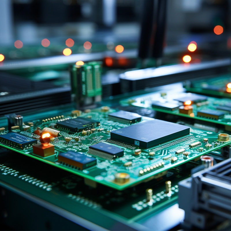
1. Substrate: The base material on which the circuit is printed, usually made of fiberglass or composite epoxy.
2. Conductive Traces: Thin copper lines that connect the components on the 2.4 ghz yagi pcb antenna.
3. Pads: Small copper areas on the PCB surface where components are soldered.
4. Vias: Holes drilled through the PCB to connect the different layers of the circuit.
5. Solder Mask: A layer of protective material that covers the copper traces and pads, preventing accidental short circuits.
6. Silkscreen: A layer of ink that is printed on the PCB to label the components and provide other useful information.
7. Components: Electronic devices such as resistors, capacitors, and integrated circuits that are mounted on the PCB.
8. Mounting Holes: Holes drilled on the PCB to allow it to be securely attached to a larger device or enclosure.
9. Copper Pour: Large areas of copper that are used to provide a common ground or power plane for the circuit.
10. Edge Connectors: Metal contacts on the edge of the PCB that allow it to be connected to other circuits or devices.
11. Solder Bridges: Small areas of exposed copper that allow for the connection of two or more traces.
12. Test Points: Small pads or holes on the PCB that allow for testing and troubleshooting of the circuit.
13. Silkscreen Legend: Printed text or symbols on the silkscreen layer that provide additional information about the PCB and its components.
14. Designators: Letters or numbers printed on the silkscreen layer to identify specific components on the PCB.
15. Reference Designators: A combination of letters and numbers that identify the location of a component on the PCB according to the schematic diagram.

Tags:2.4 ghz pcb trace antenna,1.27 mm pcb,12 layer pcb,1 oz pcb copper thickness

