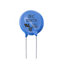
Understanding the specific demands concerning varistors in PCB assembly (PCBA) design is essential. Here’s a breakdown of what PCBA design demands from varistors:

Operating Temperature/Storage:

Maintain the working temperature of the circuit within the specified range outlined in the product’s specifications. After assembly, store the circuit within the product’s specified temperature range when it’s not operational. Avoid using temperatures higher than the specified maximum operating temperature.

Operating Voltage:

Keep the voltage applied across the varistor terminals below the maximum permissible voltage. Incorrect usage might result in product failure, short circuits, or potential heating issues. Although the usage voltage should be below the rated voltage, in cases of continuous high-frequency or pulse voltage, thoroughly assess the varistor’s reliability.

Component Heating:

Ensure that the surface temperature of the varistor remains below the highest specified operating temperature (considering temperature elevation caused by the component’s self-heating) as dictated in the product specifications. Confirm varistor temperature elevation due to circuit conditions under the actual operational state of the equipment.

Restricted Usage Areas:

  • Varistors shouldn’t be used in the following environments:
  • Places with water or saltwater.
  • Areas prone to condensation.
  • Locations with corrosive gases (such as hydrogen sulfide, sulfur dioxide, ammonia, etc.).
  • Conditions where the vibration or shock exceeds the specified range in the product specifications.

PCB Selection:

The performance of aluminum oxide circuit boards may deteriorate due to thermal shock (temperature cycling). It’s crucial to confirm if the circuit board affects the product quality during use.

Pad Size Setting:

More soldering leads to increased pressure on the varistor, leading to quality issues like surface cracks. Therefore, when designing the solder pad on the circuit board, suitable shapes and sizes must be set according to the soldering volume. Maintain an equal size for the solder pads. Uneven solder volumes on the left and right pads can cause delayed solidification on the side with more solder, leading to stress-induced cracks on the other side during solder cooling.

Component Configuration:

Installing varistors in PCBA or subjecting circuit boards to bending during operation may result in varistor fractures. Hence, configuring components must consider the circuit board’s resistance to bending and avoid applying excessive pressure.

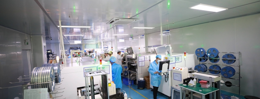
In the daily production process, meticulous attention to various production details is crucial to ensuring superior manufacturing quality. Adhering strictly to stipulated requirements with a dedicated and responsible approach during production is fundamental for lean processing, which is pivotal for the sustenance of business growth. Below, our team at the SMT Mounting Factory in MTI PCBA has compiled a guide to key considerations during SMT assembly processes. Let’s delve into it together:

Workshop Temperature and Humidity

Maintaining optimal conditions in the production workshop is essential. For SMT workshops, the ideal temperature is 24±2℃, with humidity levels around 40±10%RH. Extreme temperatures can lead to soldering issues like tin beads or solder bubbles and stencil-related problems during printing.

Material Storage

Pre-SMT assembly, the storage conditions of materials often get overlooked. For instance, PCBs exposed to air for extended periods tend to absorb moisture, resulting in poor soldering later on. Additionally, special attention is required for the storage of BGA and IC chips, necessitating a dry environment to prevent oxidation.

Solder Paste

Solder paste, a core material in SMT assembly, primarily comprises tin powder and flux. As flux plays a significant role in the entire soldering process, selecting high-quality solder paste is crucial. Pre-use procedures like reflow and stirring of solder paste are essential details not to be overlooked.

Soldering Process

The reflow soldering process holds a critical position in SMT assembly, directly impacting soldering quality. Surface mount soldering quality is among the most critical factors. Reflow soldering considerations typically involve oven temperature, preheating, and optimum temperatures.

Post-Reflow Quality Control (QC)

Product quality represents the factory’s reputation, and soldering quality significantly influences it. Exceptional products are essential for maintaining a competitive edge in the PCBA industry. Thus, stringent control over soldering process quality is imperative, focusing on details to avoid defects like open solder joints, solder skips, or bridging.

For more information on rapid prototyping in SMT assembly, high-end PCBA manufacturing, SMT mounting pricing, and more, feel free to explore MTI PCBA  for detailed insights.

When it comes to Surface Mount Technology (SMT) production, cases of welding failure caused by missing drill files are not uncommon.

Solder paste printing in SMT welding is a crucial and rather complex process, with data suggesting that 60-70% of defects in SMT production stem from solder paste printing.

Interestingly, these defects are not equipment-related but primarily emerge during engineering assessments and stencil optimizations. In particular, the absence of drilling files during engineering can lead to various SMT welding defects.

According to data provided by Company E’s Engineering Department at major welding factories, about 15% of SMT welding cases lack drilling layer files. This omission leads to at least one or more daily orders where customers fail to provide these essential files. It incurs significant communication costs, estimated at around 100 minutes per day and over 43 hours per month, arising from email exchanges between engineers, PMC, and customers to confirm and fulfill these requirements.

The stencil plays a pivotal role in SMT welding and requires a systematic approach beyond simple hole drilling. Understanding how to prevent tin ingress causing soldering issues, the necessity of drilling layer files for stencil design, and addressing various real-world cases are crucial.

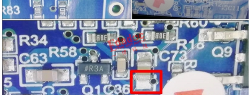
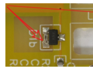
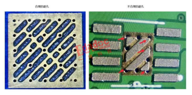
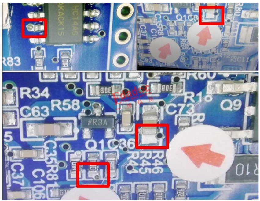
  1. For instance, issues arise when edge holes on solder pads aren’t identified due to the absence of drilling files. The consequence: unsatisfactory soldering, false soldering, and inadequate tin in resistors or connectors.

2. Similarly, the lack of avoidance holes in QFN ground solder pads results in tin ingress and false soldering. Here, it’s vital to avoid or increase tin filling in the holes to ensure sufficient coverage. Failure to provide drilling layer files prevents timely detection and avoidance of such problems during stencil creation.

Furthermore, the rush to create stencils without physical inspection of the PCB bare board can lead to issues. When customers fail to provide drilling layer files, issues such as unanticipated plate-through holes can arise during stencil creation, leading to welding anomalies.

To mitigate these concerns, it’s essential to evaluate plate-through holes for chips, maintain a distance between through-holes and SMDs, and understand the importance of resin plug-hole electroplating processes in PCB design.

In summary, by avoiding plate-through holes and ensuring the provision of drilling layer files for stencil design, welding quality can be significantly improved. This not only aids in precise hole identification but also prevents unnecessary or insufficient holes, thereby averting potential quality hazards due to poor design choices.