Comprehensive Box Build OEM Services by MTI

MTI specializes in delivering comprehensive solutions by seamlessly integrating electronics into mechanical enclosures. Our extensive experience in system integration and high-level assembly, including Build to Order (BTO) and Configure to Order (CTO), makes us a top choice for Box Build OEM services.

MTI Assembly capabilities

With a proficient engineering team and robust assembly capabilities, we are committed to meeting customer expectations for quality and reliability. Operating with six dedicated box build production lines, we offer flexible and efficient assembly for entire products.

Moreover, our fruitful 8+ years of collaboration with partners in molding, stamping, forming, and injection services ensure a reliable supply of high-quality extrusions, brackets, housings, and enclosures.

MTI’s turnkey Box Build services encompass materials procurement, PCB assembly (PCBA), final assembly manufacturing, software installation, final testing, packaging (including manuals and accessories), warehousing, and direct shipping to customers or end-users.

We manage the entire process, from sourcing mechanical components from trusted vendors to coordinating logistics, ensuring on-time delivery, competitive pricing, and uncompromised quality.

While electronics assembly may suffice for some customers, an increasing number seek comprehensive solutions, including mechanical assembly, software installation, and customized packaging.

At MTI, we provide a convenient ‘one-stop-shop’ solution for complete electronic devices. Leveraging dedicated production lines, we assemble devices, apparatus, or systems precisely to customer specifications, guided by the Bill of Material (BOM) and drawings. We can also program and pre-install software as needed.

Our Box Build service is designed to exceed customer expectations regarding quality and reliability. By overseeing the entire process, from procuring mechanical parts from our vendors or clients to coordinating logistics, we guarantee timely, cost-effective, and top-quality product delivery.

reflow soldering

Mastering Reflow Soldering: A Comprehensive Guide

Reflow soldering stands as the predominant method for attaching surface mount components onto Printed Circuit Boards (PCBs).

During the pick-and-place operation, components are situated on the board atop paste deposits. The reflow soldering process then facilitates a dependable electrical and physical connection. Solder pastes melt and subsequently cool to form robust solder joints, with the aim of achieving this without causing damage due to excessive heat.

The reflow soldering cycle typically comprises four stages: Preheat, Thermal Soak, Reflow, and Cooling.

Preheat: The oven gradually raises the temperature to heat the boards and components uniformly, paying attention to the temperature gradient to prevent component damage.

Thermal Soak: Activates flux particles, reducing oxidization, enhancing solder wetting, and promoting component longevity.

Reflow: Reaches the maximum temperature, dictated by the component with the lowest maximum temperature tolerance.

Cooling: Solder alloys solidify to form solder joints, ensuring proper wetting and preventing component damage or cold soldering.

In Reflow Soldering, quality is crucial, necessitating high-quality materials and meticulous profile optimization. Despite the time and effort invested in setting up an ideal Reflow Solder Profile for each assembly, it’s essential to achieve consistently reliable results.

MTI PCBA is a distinguished high-tech enterprise, specializing in PCB design, manufacturing, and assembly services. Committed to delivering top-notch services, MTI PCBA serves a diverse range of markets, including medical equipment, telecommunications, automotive manufacturing, and more.

FPCB

Understanding Flexible Printed Circuit Boards (FPCBs)

Flexible Printed Circuit Boards (FPCBs) are the backbone of modern flexible electronics. These boards are crafted by mounting electronic components onto flexible plastic substrates, including polyimide, PEEK, and transparent conductive polyester. FPCBs offer unparalleled advantages, such as exceptional flexibility, reduced weight, and minimal thickness, making them indispensable in contemporary electronics.

Key Components of a Flexible PCB (FPCB)

Similar to rigid PCBs, FPCBs come in single-layer, double-layer, or multi-layer configurations, comprising crucial elements:

Dielectric Substrate Film: Serving as the PCB’s foundation, polyimide (PI) is the most prevalent material, known for its impressive resistance to both tension and high temperatures.

Electrical Conductors: Copper is utilized for these conductors, delineating the circuit’s traces.

Protective Finish: A protective layer, crafted from cover lay or cover coat, safeguards the circuit.

Adhesive Material: Typically made from polyethylene or epoxy resin, this material bonds different circuit components.

Expanding the Possibilities with FPCBs

Can FPCBs revolutionize the entire electronics industry? The answer is a resounding “potentially.” While flexible displays have piqued our interest, their widespread adoption has encountered some roadblocks.

Challenges and Considerations

Designers have explored using FPCBs as substrates for motherboards, yet certain limitations persist:

Cost Increase: FPCBs can be costlier than their rigid counterparts.

Handling Risk: These boards are more susceptible to damage during handling and use.

Assembly Complexity: The assembly process can be intricate.

Repair and Rework Challenges: Fixing issues in FPCBs can be challenging or even impossible.

Panel Utilization: FPCBs often result in reduced panel utilization, increasing costs.

Despite these challenges, FPCBs play a vital role as connectors in various applications with specific demands for flexibility, space constraints, and efficient production. Consumer electronics like cell phones, cameras, and personal entertainment devices have readily embraced flexible circuits. Industrial and medical devices also leverage FPCBs, benefiting from their compact interconnections.

Flexible PCBs have ushered in a new era of electrical interconnection technology. Their continuous growth is driven by the demand for smaller, lighter electronic devices. These boards have the power to eliminate the need for traditional connectors and cables, enhancing connection reliability while reducing assembly time, costs, and overall device size.

However, designers must navigate the challenges posed by FPCBs. While they unlock exciting possibilities, careful consideration of their disadvantages is essential. As scientists and designers work tirelessly, we can expect FPCB technology to reach its full potential in the evolving landscape of electronics.


Mintec Innovation: Your One-Stop Solution for Electronic Manufacturing Service

Are you looking for a professional and reliable company that can handle your electronic manufacturing needs? Do you need a company that can provide you with schematic design, pcb layout, pcba prototype, pcba (pcb assembly) and box build assembly? If yes, then you have come to the right place. Mintec Innovation is your one-stop solution for electronic manufacturing service.

Mintec Innovation is a company that specializes in electronic manufacturing service, or EMS. EMS is the process of designing, developing, testing, and assembling electronic products or components. EMS can cover a wide range of applications, such as consumer electronics, industrial equipment, medical devices, automotive systems, aerospace products, and more.

Mintec Innovation offers a comprehensive range of EMS services, including:

• Schematic design: This is the process of creating a graphical representation of the electrical connections and components of an electronic product or circuit. Schematic design helps to define the functionality and specifications of the product or circuit.

• PCB layout: This is the process of designing the physical arrangement and placement of the components and traces on a printed circuit board. PCB layout helps to optimize the performance and reliability of the product or circuit.

• PCBA prototype: This is the process of creating a small-scale version of the product or circuit for testing and evaluation purposes. PCBA prototype helps to verify the feasibility and functionality of the product or circuit before mass production.

• PCBA (PCB assembly): This is the process of soldering the components onto the printed circuit board according to the PCB layout. PCBA (PCB assembly) helps to produce the final product or circuit that can be used or sold.

• Box build assembly: This is the process of assembling the PCBA (PCB assembly) into a complete product that includes a casing, wiring, connectors, switches, labels, etc. Box build assembly helps to provide a finished product that can be delivered to the end-user or customer.

Mintec Innovation has a team of experienced and skilled engineers, technicians, and operators who can handle any EMS project with high quality and efficiency. Mintec Innovation also has advanced equipment and facilities that can support any EMS project with high speed and accuracy. Mintec Innovation can provide you with customized solutions that meet your specific requirements and expectations.

Mintec Innovation has been in the EMS industry for over 10 years, and has served many satisfied customers from various sectors and regions. Mintec Innovation has earned a reputation for being a trustworthy and dependable partner for EMS projects. Mintec Innovation can guarantee you:

• Competitive pricing: Mintec Innovation can offer you affordable and reasonable prices for your EMS projects without compromising on quality or service.

• Rapid lead times: Mintec Innovation can deliver your EMS projects within your desired time frame without delaying or compromising on quality or service.

• High quality: Mintec Innovation can ensure that your EMS projects meet or exceed your quality standards and expectations without compromising on performance or functionality.

• Quick responsiveness: Mintec Innovation can communicate with you effectively and efficiently throughout your EMS projects without compromising on clarity or transparency.

If you are interested in working with Mintec Innovation for your EMS projects, please feel free to contact us today. We will be happy to discuss your needs and provide you with a free quote. You can also visit our website [Mintec Innovation] to learn more about our services and capabilities.

Thank you for reading this article. We hope that you have learned more about Mintec Innovation and our electronic manufacturing service.

MTI PCBA’s Expertise Unveiled: Pioneering the Future of Sleep with MindLax

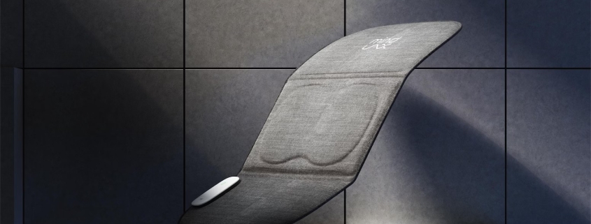
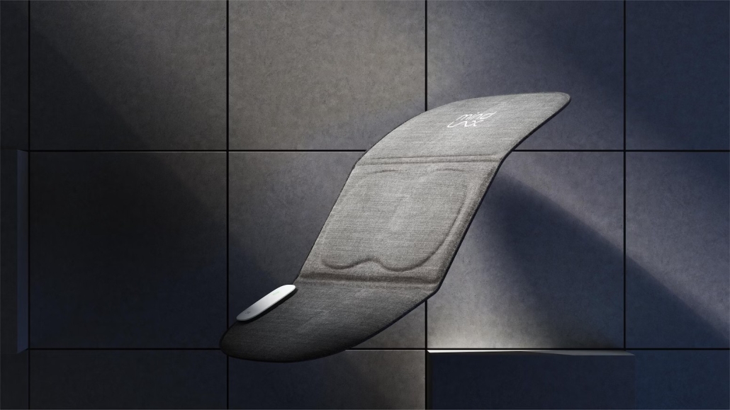
In today’s fast-paced world, quality sleep is a precious commodity that many struggle to obtain. Recognizing the importance of restful nights, MTI PCBA has taken the lead in pioneering an innovative sleep solution: the MindLax Sleeping Mat. This revolutionary tool, engineered from the ground up by MTI PCBA’s experienced team, promises to transform the way we approach sleep.

The Birth of MindLax

Quality sleep is a fundamental component of our overall well-being, impacting our physical health, mental acuity, and emotional stability. With this understanding, MTI PCBA embarked on a journey to develop a groundbreaking sleep aid that would revolutionize the way we experience rest.

MindLax emerged from the fusion of cutting-edge technology and scientific understanding of sleep patterns. At its core, it utilizes aviation-grade special rare metal materials and pairs them with digital content and a sophisticated algorithm to optimize its effectiveness.

MTI PCBA’s Role in MindLax’s Journey

MTI PCBA is the driving force behind the creation of MindLax, taking charge of every stage of development, from inception to mass production. Let’s delve into the remarkable capabilities and experiences that make MTI PCBA the ideal partner for such an ambitious project.

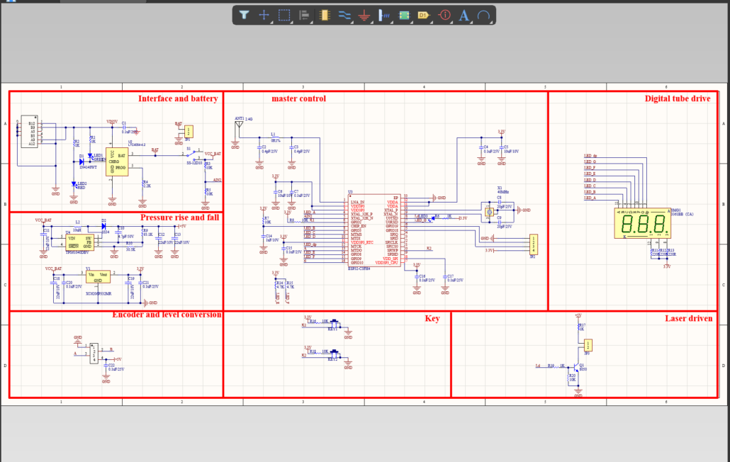
1. Schematic Design: The Blueprint for Innovation

The journey began with the creation of a comprehensive schematic design that laid the foundation for MindLax’s exceptional capabilities. MTI PCBA’s team of skilled engineers meticulously crafted the blueprint, ensuring that every component would seamlessly interact to achieve the desired sleep-enhancing effects.

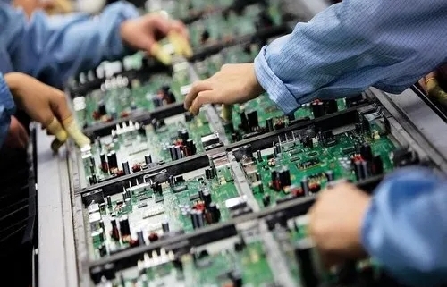
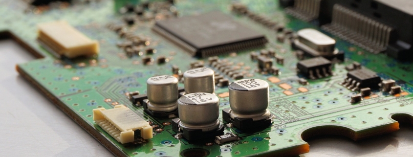
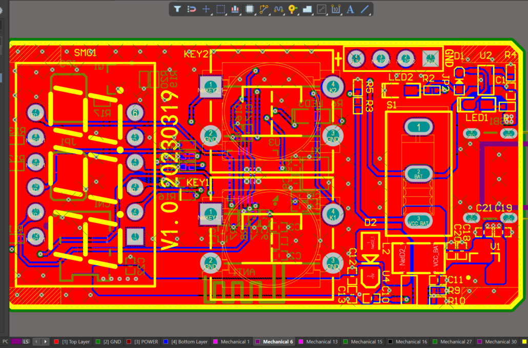
2. PCB Layout: Precision in Every Detail

The printed circuit board (PCB) is the nervous system of MindLax, connecting its various components and facilitating communication. MTI PCBA‘s expertise in PCB layout was instrumental in designing a compact yet efficient board that maximized MindLax’s functionality while maintaining user comfort.

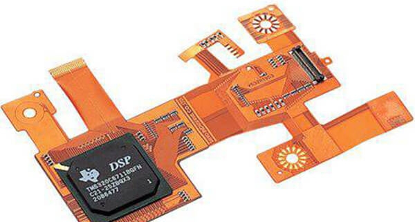
3. Firmware Development: Bringing MindLax to Life

MindLax’s capabilities extend beyond hardware. Its firmware, developed by MTI PCBA‘s proficient team, enables seamless operation and synchronization of its multi-frequency waveguide system. The firmware’s efficiency ensures that users can harness MindLax’s potential effortlessly.

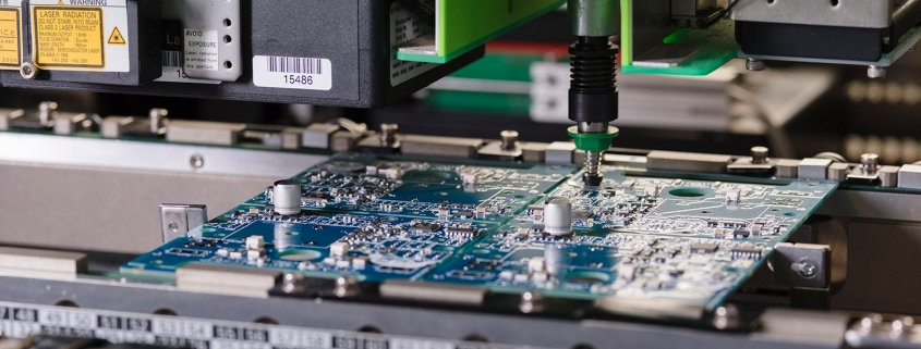
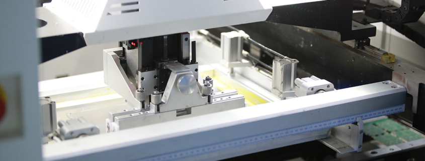
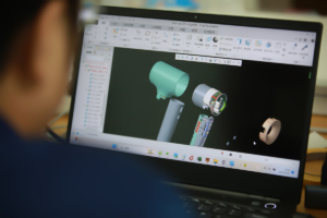
4. Prototyping: Iterative Perfection

Before unveiling the final product, extensive prototyping was necessary to fine-tune MindLax’s performance. MTI PCBA‘s commitment to perfection drove a series of iterations and improvements, resulting in a sleep aid that consistently delivers on its promises.

MindLax Controlboard.

PCBA

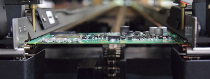
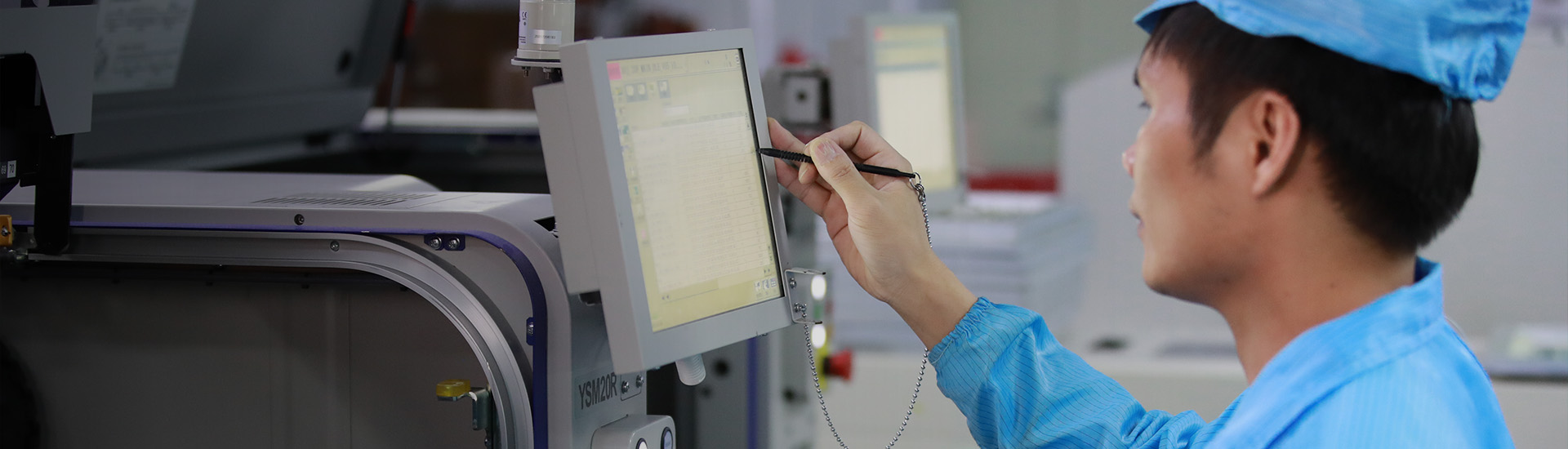
5. Mass Production: Scaling Sweet Dreams

MTI PCBA’s ability to transition from prototype to mass production is a testament to its manufacturing prowess. This transition ensures that MindLax is readily available to help people worldwide experience the benefits of improved sleep.

MindLax’s Unique Features

Central to MindLax’s effectiveness is its Multi-frequency Waveguide System, which incorporates two essential elements: Neuro TIM™️ and Neuro Arc™️. Together, these components transmit sleep-enhancing sounds and vibrations directly to the brain, bolstering the production of Alpha brain waves—a key factor in achieving high-quality sleep.

– Neuro TIM™️: The Brainwave Maestro

Neuro TIM™️ is the conductor of MindLax’s symphony of sleep. Through carefully crafted soundscapes and vibrations, it orchestrates the brain’s Alpha wave production. These Alpha waves are instrumental in achieving deep relaxation and fostering a tranquil state of mind conducive to restful sleep.

– Neuro Arc™️: The Path to Rapid Relaxation

Neuro Arc™️ complements Neuro TIM™️ by ensuring rapid and profound relaxation. Its innovative approach leverages advanced algorithms and digital content to guide users into a state of deep relaxation swiftly. This groundbreaking combination sets the stage for restorative sleep.

The Future of Sleep with MindLax

The introduction of MindLax marks a significant milestone in the quest for improved sleep quality. MTI PCBA‘s unwavering commitment to innovation, precision, and excellence has culminated in a product that promises to redefine the way we sleep.

As MindLax continues to gain recognition for its transformative effects, it also serves as a testament to MTI PCBA‘s capabilities and dedication to pushing the boundaries of what is possible in the world of electronic design and manufacturing.

In conclusion, MindLax represents a harmonious union of technology, science, and ingenuity, with MTI PCBA as its visionary architect. Together, they have created a sleep solution that empowers individuals to unlock the full potential of restful nights, contributing to healthier, happier lives.

Discover the future of sleep with MindLax—a testament to MTI PCBA‘s passion for innovation and excellence.

PCBA

Understanding the PCBA (Printed Circuit Board Assembly) Process

Introduction:

PCBA, which stands for Printed Circuit Board Assembly, is a crucial step in the manufacturing of electronic devices. It involves attaching electronic components to a printed circuit board (PCB) to create a functional electronic circuit. This intricate process forms the backbone of modern electronics manufacturing, and here, we delve into the various stages involved.

PCBA Process:

Solder Paste Stenciling:

After the bare PCB is fabricated, solder paste is applied to the pads for Surface Mount Technology (SMT).
Solder paste, composed of tin, silver, and copper, facilitates physical and electrical connections between components and the board.
A precise machine applies solder paste evenly, guided by a stencil tailored to the PCB layout.

Pick and Place:

A robotic pick-and-place machine rapidly positions Surface Mount Devices (SMDs) on the PCB.
These machines are programmed for specific projects, ensuring accurate component placement.
As components shrink in size, specialized machines handle the tiniest SMDs.

Reflow Soldering:

Once components and solder paste are in place, the PCB undergoes reflow soldering.
The board is heated in stages to 250°C, melting the solder paste and solidifying it as it cools.
This controlled process ensures secure component attachment.

Inspection and Quality Control:

After SMT, a thorough inspection checks physical and electrical connections.
Automatic Optical Inspection (AOI) machines use cameras to identify solder joint quality.
Defective boards are reworked or discarded based on quality standards.

Through-Hole Component Insertion:

Plated Through-Holes (PTH) are utilized when necessary for components.
These holes enable signals to pass through the board.
Workers manually insert PTH components into the board.

Wave Soldering:

Wave soldering is employed for mass production, eliminating hand soldering.
Boards move through a wave solder machine, where a molten solder wave solders the PTH components’ joints.
Care must be taken with double-sided PCBs to prevent damage.

Final Inspection and Functional Test:

The PCB undergoes a functional test simulating real-world conditions.
Electrical characteristics, such as voltage, current, and signal output, are examined.
Any deviations from predetermined ranges indicate a failed PCB.

Cleaning:

After assembly, residual solder paste, oils, and contaminants are removed.
High-pressure washing with deionized water ensures a clean board.
The PCB is dried and prepared for packaging.


The PCBA process is the backbone of electronic manufacturing, ensuring the creation of reliable and functional electronic devices. Each stage, from soldering to testing, plays a vital role in producing high-quality PCBAs that power our modern world. Understanding this process sheds light on the complexity and precision required in electronics manufacturing.

Empowering Connectivity: The Evolution of 5G CPE Technology

5G CPE, or 5G Customer Premise Equipment, is a device that connects to a 5G network and provides internet access to other devices via Wi-Fi or Ethernet. 5G CPE can offer faster and more reliable internet service than traditional routers or modems, as it can support higher bandwidth, lower latency, and wider coverage. In this article, we will share our development experience for 5G CPE, from schematic design to PCB assembly.

Schematic Design

The first step of our development process was to design the schematic of the 5G CPE device. The schematic is a graphical representation of the electrical connections and components of the device. The schematic shows how the power supply, the 5G module, the Wi-Fi module, the Ethernet module, the antenna, and other parts are connected and configured. The schematic also specifies the values and ratings of the resistors, capacitors, inductors, diodes, transistors, and other components.

To design the schematic, we used [EAGLE], a software tool that allows us to create and edit schematic diagrams easily and efficiently. EAGLE has a library of thousands of standard components that we can drag and drop into our schematic. EAGLE also has a simulation feature that allows us to test and verify our schematic before moving on to the next step.

PCB Layout

The second step of our development process was to design the PCB layout of the 5G CPE device. The PCB layout is a physical representation of the arrangement and placement of the components and traces on the printed circuit board. The PCB layout shows how the components are mounted on the board, how the traces are routed between them, and how the board is shaped and sized.

To design the PCB layout, we used [KiCad], a software tool that allows us to create and edit PCB layouts easily and efficiently. KiCad has a feature that allows us to import our schematic from EAGLE and automatically generate a PCB layout based on it. KiCad also has a 3D viewer that allows us to see how our PCB layout looks like in real life.

PCB Assembly

The third and final step of our development process was to assemble the PCB of the 5G CPE device. The PCB assembly is the process of soldering the components onto the printed circuit board according to the PCB layout. The PCB assembly requires precision and accuracy, as any mistake or defect can affect the performance or functionality of the device.

To assemble the PCB, we used [JLCPCB], a professional PCB manufacturer that offers high-quality PCB assembly services at low prices. JLCPCB has a feature that allows us to upload our PCB layout file and order our PCBs online. JLCPCB also has a large inventory of standard components that we can choose from for our PCB assembly. JLCPCB can deliver our assembled PCBs within a few days.

We have successfully developed 5G CPE from schematic design to PCB assembly using various software tools and services. We have learned a lot from this project, and we are proud of our achievement. We hope that our development experience can inspire and help others who are interested in creating their own 5G CPE devices. If you have any questions or feedback, please feel free to contact us. Thank you for reading.


Mintec’s expert PCB fabrication services ensure top-notch electronic solutions. With cutting-edge technology and meticulous attention to detail, we offer high-quality, cost-effective PCBs for various applications. Our team excels in quick turnarounds, meeting diverse specifications, and producing complex PCB designs. From prototypes to large-scale production, we ensure reliability and precision. Trust in Mintec’s decades of experience in the industry, ensuring your electronic projects achieve optimal performance. Let us be your partner in realizing innovative and efficient PCB solutions.


With Mintec’s extensive expertise in PCB fabrication, we cater to diverse industries, including automotive, aerosp
ace, telecommunications, and consumer electronics. Our state-of-the-art facilities and skilled workforce enable us to handle both low and high volum
e orders without compromising on quality or delivery time. From single-layer to multi-layer boards, we tailor our services to meet your specific requirements. Mintec is committed to customer satisfaction, ensuring seamless communication, and delivering precision-engineered PCBs that exceed expectations. Experience the difference with Mintec’s reliable and innovative PCB fabrication solutions.