As a comprehensive PCBA manufacturer, we aim to shed light on the significance and nuances of OSP (Organic Solderability Preservatives) surface finishing in PCB manufacturing. OSP, or Organic Solderability Preservatives, also known as Copper Protective Agent, is a widely-used surface treatment method that shields exposed copper from air during PCB fabrication. However, as with any technology, OSP comes with its own set of strengths and limitations. Let’s explore the advantages and disadvantages of this surface treatment technique in PCBA.

Advantages of OSP:

OSP serves as a protective barrier between copper and air. Its organic nature sets it apart, making it a cost-effective alternative compared to other treatments like tin-spraying processes. The principle involves chemically cultivating a thin organic film on a clean bare copper surface, often found in computer motherboards.

However, there are drawbacks to consider:

OSP’s transparency and lack of color make visual inspection challenging; distinguishing whether OSP treatment has been applied becomes difficult.

OSP’s non-conductive nature interferes with electrical testing, necessitating the removal of the OSP layer using tin paste via stencil printing to facilitate these tests.

OSP is susceptible to corrosion and vulnerable to acid and temperature influences. Prolonged storage or exposure can require re-surface treatment.

An OSP-treated board exposed to air for around ten days becomes unsuitable for component soldering.

This insight provides an overview of OSP surface treatment’s roles and its pros and cons in PCB fabrication. For deeper insights, don’t hesitate to get in touch with MTI PCBA.

How to Prevent PCB Warping in PCBA Manufacturing during SMT Process

During the Surface Mount Technology (SMT) manufacturing process, Printed Circuit Boards (PCBs) can experience warping, leading to various defects such as component misalignment and tombstoning. In this article, we will discuss effective methods employed by Shenzhen PCBA manufacturers to prevent PCB warping during PCBA manufacturing:

1. Temperature Control:

Managing temperature is vital because it is the primary source of stress for PCBs. Reducing the temperature in the reflow oven or adjusting the heating and cooling rates during the reflow process can significantly mitigate PCB warping. However, this approach must be carefully balanced, as lower temperatures may lead to issues like solder bridging.

2. High Tg Materials:

Tg, or glass transition temperature, represents the point at which a material shifts from a solid, glassy state to a rubbery state. Materials with lower Tg values soften more rapidly during reflow and remain in a rubbery state for a more extended period. This can result in more severe board deformation. To enhance a PCB’s ability to withstand stress-induced deformation, manufacturers can opt for materials with higher Tg values, although this choice may come at a higher cost.

3. Board Thickness Increase:

Many electronic devices aim for slim designs, resulting in PCB thicknesses as low as 1.0mm, 0.8mm, or even 0.6mm. These ultra-thin boards are more susceptible to deformation during reflow soldering. If slimness is not a strict requirement, it is advisable to use PCBs with a thickness of 1.6mm. This significantly reduces the risk of PCB warping and deformation.

4. Dimension and Panelization Management:

Since most reflow ovens use chain conveyors to transport PCBs, larger boards are more prone to sagging or deformation due to their own weight. To minimize deformation, it is recommended to orient the longer side of the board parallel to the conveyor chain. Furthermore, reducing the number of panels during reflow soldering, by positioning narrow sides perpendicular to the conveyor direction, aids in minimizing deformation.

5. Reflow Soldering Carriers or Fixtures:

When other methods prove challenging, using reflow soldering carriers or fixtures can be the solution to minimize PCB deformation. These fixtures, usually constructed from materials like aluminum alloy or synthetic stone, are known for their high-temperature resistance. They stabilize the PCB during high-temperature expansion and subsequent cooling, preserving the PCB‘s original dimensions until the temperature drops below the Tg point. At this stage, the PCB regains its rigidity. In cases where single-layer fixtures are insufficient, double-layer fixtures with a cover can further reduce PCB deformation. However, it’s worth noting that such fixtures can be costly and require additional labor for setup and removal.

6. Router for Depanelization:

As V-Cut may weaken the structural integrity of panelized PCBs, it’s advisable to avoid V-Cut or minimize its depth.

These methods play a critical role in helping PCB manufacturers prevent PCB warping issues during the SMT manufacturing process, ensuring the production of high-quality Printed Circuit Board Assemblies (PCBAs). For more info. Please contact MTI PCBA.

PCBAs are intricate assemblies with numerous components and solder connections. To ensure their flawless performance, In-Circuit Testing (ICT) is vital. ICT assesses individual components and electronic characteristics for imperfections. It’s a longstanding, dependable testing method in electronics.

PCBA ICT Testing

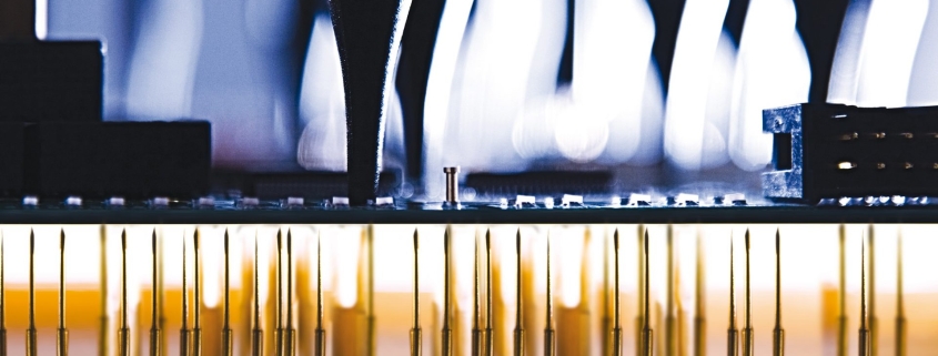
ICT, or In-Circuit Testing, detects defective components using electrical probes to check specific points on the board. It examines shorts, opens, resistance, capacitance, and more. This automated process allows for immediate repair or replacement of faulty parts.

Advantages of PCBA ICT Testing

  • Detects manufacturing defects such as component spacing, soldering, shorts, and more.
  • Easy to program using PCB layout files.
  • Results are straightforward to interpret.
  • Disadvantages of ICT Testing

Requires expensive test fixtures.

May struggle with connector faults in small components.
Results vary if test pins don’t make proper contact.
Regular pin maintenance is essential.
Despite its drawbacks, ICT remains one of the best PCBA testing methods. It’s efficient, and our experienced team at Auspi can assist you with your project.