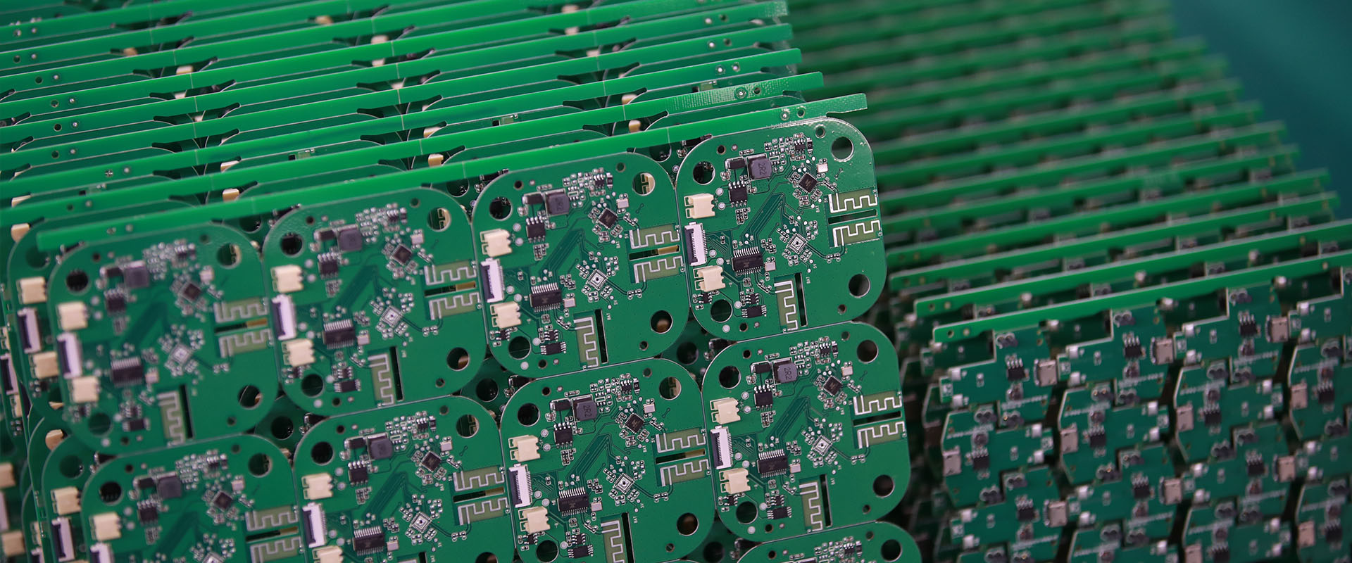
In today’s fast-paced electronics industry, high-volume PCB manufacturing is essential to meet the growing demand for reliable and cost-effective electronic components. MTI, a leading printed circuit board manufacturer, specializes in delivering high-quality PCB tailored for large-scale production. This article explores the features and benefits of MTI’s PCB manufacturing capabilities and how they cater to high-volume production needs.

The Importance of High-Volume PCB Manufacturing

High-volume PCB manufacturing is crucial for industries that require large quantities of electronic components quickly and efficiently. This includes sectors like consumer electronics, automotive, telecommunications, and industrial automation, where consistency, quality, and rapid delivery are paramount.

Key Features of MTI’s High-Volume PCB Manufacturing

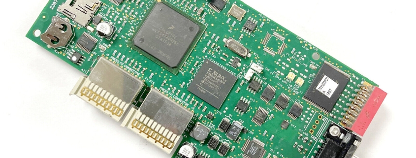
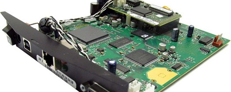
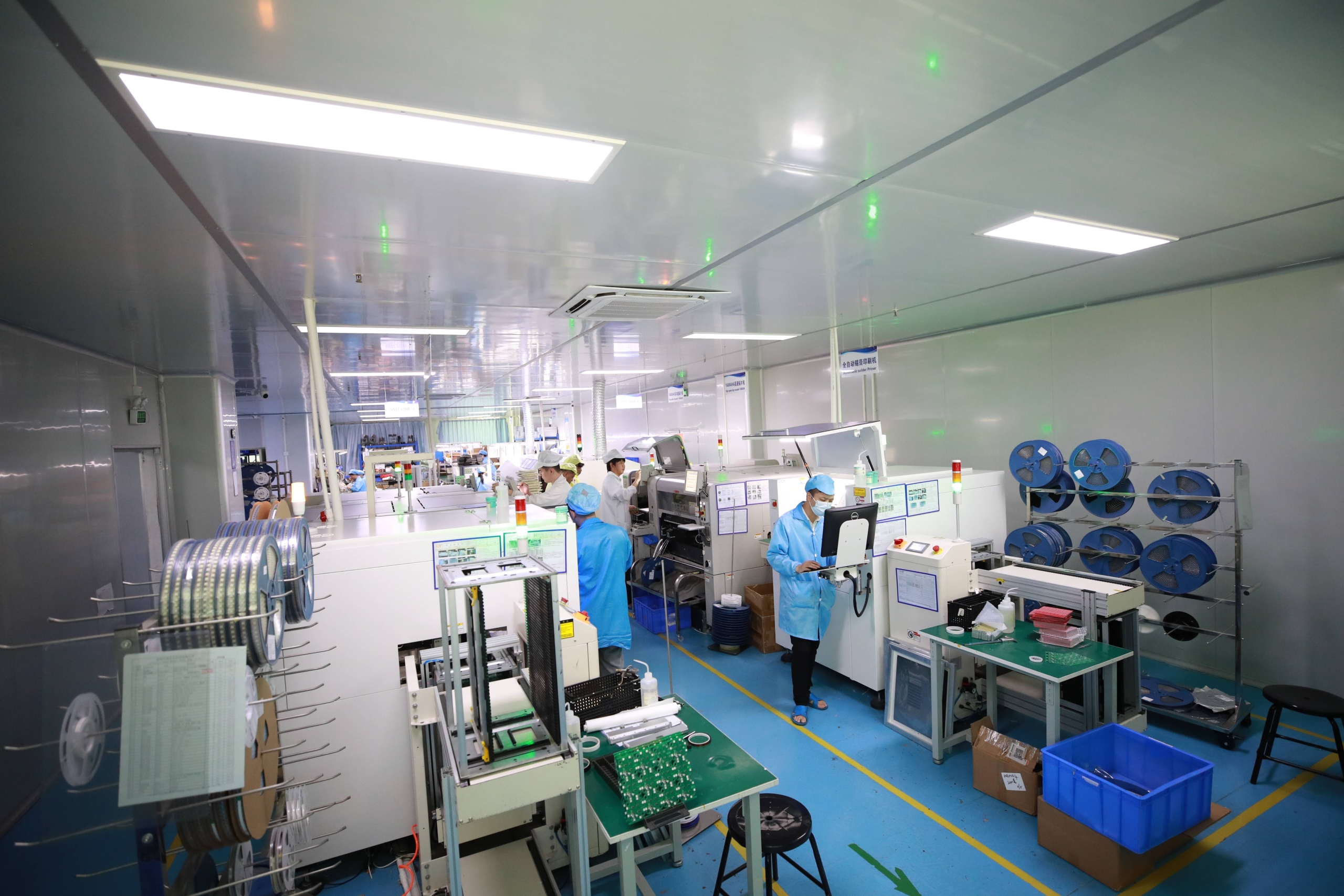
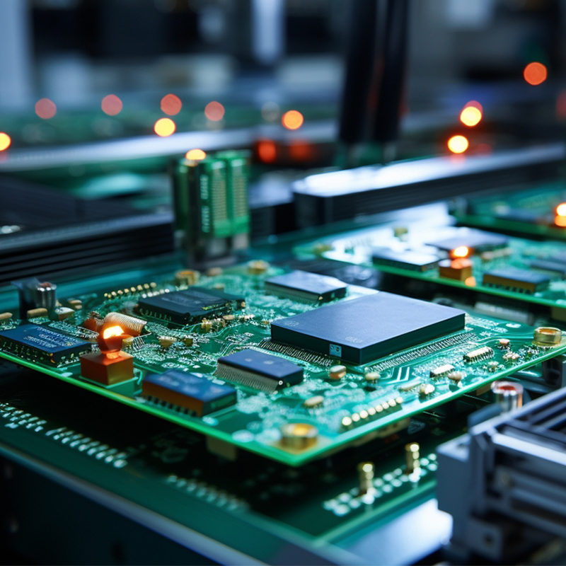
1. State-of-the-Art Manufacturing Facilities: MTI’s manufacturing facilities are equipped with advanced machinery and technology to handle large-scale PCB production. This ensures high precision and consistency across all units.

2. Efficient Production Processes: MTI utilizes lean manufacturing principles to streamline production processes, reduce waste, and improve efficiency. This results in faster turnaround times and cost savings for high-volume orders.

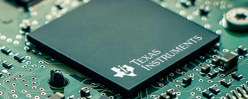
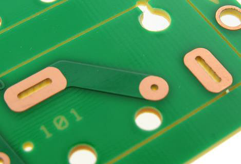
3. High-Quality Materials: MTI sources high-quality materials to ensure the durability and performance of their PCB. These materials meet strict industry standards, guaranteeing reliability and longevity in various applications.

Benefits of MTI’s High-Volume PCB Manufacturing

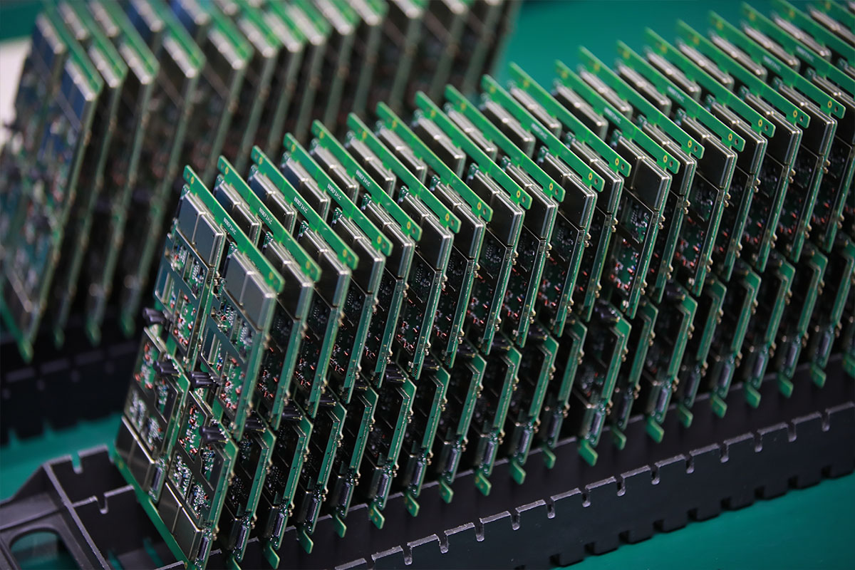
1. Scalability: MTI’s manufacturing capabilities allow for easy scalability, making it possible to ramp up production quickly in response to increasing demand. This is particularly advantageous for industries that experience seasonal spikes or sudden market shifts.

2. Cost Performance: MTI focuses on providing excellent cost performance by optimizing production processes and using high-quality materials. This ensures competitive pricing without compromising on quality, making it an attractive option for businesses looking to maximize their ROI.

3. Customizable Solutions: MTI offers customizable PCB solutions for OEM/ODM projects, allowing clients to tailor the design to their specific needs. This flexibility ensures that each PCB meets the unique requirements of its intended application.

The MTI Advantage

As a leading Chinese manufacturer, MTI offers several key advantages:

1. Expertise in Manufacturing: With extensive experience in PCB manufacturing, MTI combines traditional craftsmanship with modern technology to deliver superior PCB that meet international standards.

2. Innovative R&D: Continuous research and development efforts ensure that MTI stays ahead of industry trends and incorporates the latest advancements into their products. This commitment to innovation keeps MTI at the forefront of the PCB industry.

3. Comprehensive Support: From initial design consultation to after-sales service, MTI provides comprehensive support to their clients. Their team of experts is always available to assist with technical inquiries and ensure customer satisfaction.

Applications of MTI’s High-Volume PCB

MTI’s PCB are suitable for a wide range of applications, including:

– Consumer Electronics: High-volume production of PCB for smartphones, tablets, and other consumer devices.
– Automotive: Reliable PCB for automotive electronics, including infotainment systems, sensors, and control units.
– Telecommunications: Advanced PCB for networking equipment, routers, and communication devices.
– Industrial Automation: Durable PCB for industrial machinery, control systems, and automation solutions.

Conclusion

High-volume PCB manufacturing is essential for meeting the growing demands of various industries. MTI, a renowned printed circuit board manufacturer, offers advanced solutions that cater to large-scale production needs. By leveraging state-of-the-art facilities, efficient production processes, and high-quality materials, MTI ensures that their PCB deliver superior performance, reliability, and cost efficiency.

In the dynamic field of IoT, the ESP8266 microcontroller has gained popularity for its robust WiFi capabilities and ease of integration. MTI, a leading PCBA assembly manufacturer, offers advanced PCB integration solutions tailored to optimize the performance and connectivity of the ESP8266 pinout. This article explores the features and benefits of MTI’s PCB integration for the ESP8266 pinout and how it can enhance your IoT projects.

The Significance of PCB Integration for ESP8266

Effective PCB integration is crucial for maximizing the connectivity and performance of the ESP8266 microcontroller. A well-designed PCB ensures efficient signal transmission, minimizes interference, and provides a stable platform for IoT applications, making it indispensable for achieving optimal functionality.

Key Features of MTI’s PCB Integration for ESP8266 Pinout

1. Precision Design: MTI’s PCBs are meticulously designed to accommodate the ESP8266 pinout, ensuring accurate alignment and connectivity. The precision design minimizes signal loss and enhances the overall performance of the IoT device.

2. High-Quality Materials: MTI uses top-grade materials in their PCB manufacturing process. These materials are carefully selected to ensure durability, reliability, and excellent electrical performance, meeting the high standards required for IoT applications.

3. Customizable Solutions: MTI offers customizable PCB solutions for OEM/ODM projects. This flexibility allows clients to tailor the design to their specific requirements, ensuring that the PCB meets the unique needs of their application.

Benefits of Using MTI’s PCB Integration for ESP8266

1. Enhanced Connectivity: The precise design and high-quality materials used in MTI’s PCBs ensure robust and reliable connectivity for the ESP8266. This enhanced connectivity is crucial for maintaining stable and efficient communication in IoT networks.

2. Improved Cost Performance: MTI focuses on providing excellent cost performance by optimizing their manufacturing processes and using high-quality materials. This ensures that clients receive durable and efficient PCBs at competitive prices.

3. Scalability and Flexibility: MTI’s customizable solutions allow for scalability and flexibility in IoT projects. Whether you need to expand your network or adapt to new requirements, MTI’s PCBs can be tailored to meet evolving needs.

The MTI Advantage

As a leading Chinese manufacturer, MTI provides several key advantages:

1. Expertise in Manufacturing: With extensive experience in PCBA assembly, MTI combines traditional craftsmanship with modern technology to produce superior PCBs that meet international standards.

2. Innovative R&D: Continuous research and development efforts ensure that MTI stays ahead of industry trends and incorporates the latest advancements into their products. This commitment to innovation keeps MTI at the forefront of the PCB industry.

3. Comprehensive Support: From initial design consultation to after-sales service, MTI provides comprehensive support to their clients. Their team of experts is always available to assist with technical inquiries and ensure customer satisfaction.

Applications of MTI’s PCBs with ESP8266

MTI’s PCBs optimized for the ESP8266 pinout are suitable for a wide range of IoT applications, including:

– Smart Home Devices: Enhancing connectivity and functionality in smart home systems.
– Industrial Automation: Improving efficiency and communication in automated industrial processes.
– Wearable Technology: Providing reliable and compact solutions for wearable devices.
– Healthcare Devices: Enabling advanced connectivity and data management in medical equipment.

Conclusion

Maximizing connectivity is essential for the success of IoT projects, and MTI’s PCB integration solutions for the ESP8266 pinout are designed to achieve this goal. By leveraging precision design, high-quality materials, and customizable solutions, MTI ensures that your IoT devices benefit from enhanced connectivity, reliability, and cost performance.

In the rapidly evolving world of IoT, integrating advanced technologies like the ESP32 WiFi Marauder into PCB design can significantly enhance the capabilities and performance of your projects. MTI, a leading PCB manufacturer, offers high-quality PCBs optimized for the ESP32 WiFi Marauder, ensuring seamless integration and superior functionality. This article explores the features and benefits of using ESP32 WiFi Marauder on MTI’s PCBs and how it can elevate your IoT projects.

The Power of ESP32 WiFi Marauder

The ESP32 WiFi Marauder is a powerful and versatile microcontroller that combines WiFi and Bluetooth capabilities, making it ideal for a wide range of IoT applications. Its high processing power, low energy consumption, and rich set of peripherals enable developers to create innovative and efficient IoT solutions.

Key Features of MTI’s PCB for ESP32 WiFi Marauder

1. High-Quality Materials: MTI uses top-grade materials in the manufacturing of their PCBs, ensuring durability and reliable performance. These materials are sourced from trusted suppliers and are rigorously tested to meet the highest standards.

2. Precision Design: MTI’s PCBs are designed with precision to accommodate the ESP32 WiFi Marauder’s specifications. The optimized layout and component placement ensure efficient signal transmission and minimal interference, enhancing the overall performance of your IoT projects.

3. Customizable Solutions: MTI offers customizable PCB solutions for OEM/ODM projects, allowing clients to tailor the design to their specific requirements. This flexibility ensures that each PCB meets the unique needs of the intended application.

Benefits of Using ESP32 WiFi Marauder on MTI’s PCB

1. Enhanced Connectivity: The ESP32 WiFi Marauder provides robust WiFi and Bluetooth connectivity, enabling seamless communication between devices. MTI’s high-quality PCBs ensure that this connectivity is maintained without interruptions, improving the reliability of your IoT system.

2. Improved Cost Performance: MTI focuses on providing excellent cost performance by optimizing the manufacturing process and using high-quality materials. This ensures that you receive a reliable and durable PCB at a competitive price, enhancing the overall value of your IoT project.

3. Scalability and Flexibility: MTI’s customizable PCB solutions allow you to scale and adapt your IoT projects as needed. Whether you require additional components or specific design modifications, MTI can accommodate your needs, providing a scalable solution for future expansions.

The MTI Advantage

As a leading Chinese manufacturer, MTI offers several key advantages:

1. Expertise in Manufacturing: With extensive experience in PCB manufacturing, MTI combines traditional craftsmanship with modern technology to deliver superior PCBs that meet international standards.

2. Innovative R&D: Continuous research and development efforts ensure that MTI stays ahead of industry trends and incorporates the latest advancements into their products. This commitment to innovation keeps MTI at the forefront of the PCB industry.

3. Comprehensive Support: From initial design consultation to after-sales service, MTI provides comprehensive support to their clients. Their team of experts is always available to assist with technical inquiries and ensure customer satisfaction.

Applications of MTI’s PCBs with ESP32 WiFi Marauder

MTI’s PCBs optimized for the ESP32 WiFi Marauder are suitable for a wide range of IoT applications, including:

– Smart Home Devices: Enhancing connectivity and functionality in smart home systems.
– Industrial Automation: Improving efficiency and communication in automated industrial processes.
– Wearable Technology: Providing reliable and compact solutions for wearable devices.
– Healthcare Devices: Enabling advanced connectivity and data management in medical equipment.

Conclusion

Integrating the ESP32 WiFi Marauder with MTI’s high-quality PCBs can significantly enhance the performance and capabilities of your IoT projects. By leveraging advanced materials, precision design, and customizable solutions, MTI ensures that your IoT devices achieve superior connectivity, reliability, and cost performance.

When it comes to printed circuit boards (PCBs) and soldering, MTI stands out as a leading PCB assembly manufacturer. With a commitment to excellence and innovation, MTI offers a comprehensive range of services, from design and R&D to manufacturing and OEM/ODM solutions. This guide will take you through the essentials of PCB and soldering, helping you understand the processes and the expertise that MTI brings to the table.

Introduction to PCBs and Soldering

PCBs are the backbone of electronic devices, providing the physical foundation and electrical connections that make technology work. Soldering is the process of joining components to the PCB, ensuring reliable and stable connections. Mastering these skills is crucial for anyone involved in electronics.

MTI: Your Trusted PCB Assembly Manufacturer

At MTI, we pride ourselves on being a top-tier PCB assembly manufacturer. Our state-of-the-art facilities and skilled workforce enable us to deliver high-quality PCBs tailored to your specific needs. Whether you require small-scale prototypes or large-scale production, we have the capabilities to meet your demands.

Comprehensive Manufacturing Services

MTI offers a complete suite of manufacturing services. Our advanced manufacturing processes ensure precision and efficiency, resulting in PCBs that meet the highest standards of quality. We utilize cutting-edge technology to optimize production and minimize errors, ensuring that your products are built to last.

OEM/ODM Solutions

As an experienced OEM/ODM provider, MTI offers customized solutions that cater to your unique requirements. We work closely with you to develop products that align with your vision and specifications. Our flexible approach allows us to adapt to different industries and applications, providing you with tailored solutions that enhance your product offerings.

Expert R&D and Design Services

Research and development (R&D) are at the heart of innovation. MTI’s dedicated R&D team is constantly exploring new technologies and methodologies to improve our services. Our design experts collaborate with you to create PCBs that meet your functional and aesthetic requirements. From concept to completion, we ensure that every detail is meticulously planned and executed.

Soldering Techniques: From Basics to Advanced

Soldering is a critical skill in PCB assembly. Here’s a breakdown of the essential techniques:

1. Basic Soldering: Understanding the fundamentals of soldering, including the types of solder and flux, is essential. Properly heating the solder joint and applying the right amount of solder are key to creating reliable connections.

2. Surface Mount Technology (SMT): SMT is widely used in modern PCB assembly. It involves placing components directly onto the PCB surface and soldering them in place. This technique allows for more compact and efficient designs.

3. Through-Hole Soldering: This traditional method involves inserting component leads through holes in the PCB and soldering them on the opposite side. It is often used for components that require a stronger mechanical bond.

4. Reflow Soldering: Used primarily for SMT, reflow soldering involves applying solder paste to the PCB, placing components, and then heating the assembly in a reflow oven. The solder melts and forms solid connections as it cools.

5. Wave Soldering: Ideal for through-hole components, wave soldering involves passing the PCB over a wave of molten solder. This method is efficient for mass production.

Conclusion

MTI’s expertise in PCB assembly and soldering ensures that you receive top-quality products tailored to your needs. Our comprehensive services, including manufacturing, OEM/ODM, R&D, and design, make us your go-to partner for all your PCB requirements. Trust MTI to deliver excellence and innovation in every project.

Explore our services today and discover how MTI can elevate your electronic products to new heights.

Tags: PCB Bog,SCHEMATIC DESIGN,PCB LAYOUT,FIRMWARE DEVELOPMENT,SMT,PCB TPH Assembly,Box Build Assembly,NPI PCBA PROTOTYPE,

The Printed Circuit Board (PCB) layout is a critical step in the design and manufacturing of electronic devices. MTI, a leading PCBA factory, supplier, and distributor, provides top-notch PCB layout services to ensure the optimal performance of electronic products. This article explores the fundamentals of PCB layout, highlighting our commitment to low-cost solutions, advanced manufacturing techniques, and customized services (OEM/ODM).

PartⅠ: Understanding PCB Layout

PCB layout refers to the arrangement of electronic components and the routing of electrical connections on a printed circuit board. It is a crucial process that impacts the performance, reliability, and manufacturability of electronic devices.

– Application: Used in various electronic devices, from simple gadgets to complex industrial machinery.
– Benefit: Ensures efficient and reliable operation of electronic circuits.

PartⅡ: High-Quality Manufacturing

At MTI, we utilize state-of-the-art technology and high-grade materials to produce top-quality PCBs. Our advanced manufacturing processes ensure that each board meets stringent quality standards.

– Manufacturing: Employing cutting-edge machinery and quality control processes.
– Benefit: Consistent quality and exceptional performance.

PartⅢ: Types of PCB

We offer a variety of PCBs tailored to different electronic applications, including:

– Single-Sided PCBs: Ideal for simple electronic devices.
– Double-Sided PCBs: Suitable for more complex circuits with components on both sides.
– Multilayer PCBs: Designed for high-density and high-performance applications.
– Flexible PCBs: Perfect for applications requiring flexibility and durability.

– Benefit: Diverse options to meet specific electronic requirements.
– Application: From consumer electronics to advanced industrial equipment.

PartⅣ: Cost-Effective Solutions

MTI is dedicated to providing low-cost solutions without compromising on quality. Our efficient manufacturing processes and bulk production capabilities ensure that our PCBs are both affordable and high-performing.

– Low Costs Solution: Advanced manufacturing techniques and economies of scale.
– Benefit: High-quality products at competitive prices.

PartⅤ: Customized Services (OEM/ODM)

We offer customized services to cater to the unique needs of our clients. Whether you require specific sizes, designs, or functionalities, our OEM/ODM services ensure that your PCBs are tailored to your exact specifications.

– Customized Services (OEM/ODM): Providing bespoke solutions to fit unique electronic needs.
– Benefit: Customizable boards that enhance product performance and customer satisfaction.

PartⅥ: The Importance of PCB Layout

1. Component Placement
Proper component placement is vital for the performance and reliability of the PCB. It ensures efficient routing, minimizes signal interference, and optimizes thermal management.

– Benefit: Improved circuit performance and reduced risk of errors.

2. Routing
Routing involves creating electrical connections between components. Effective routing minimizes the length of connections, reduces cross-talk, and ensures signal integrity.

– Benefit: Enhanced signal quality and circuit reliability.

3. Thermal Management
Efficient thermal management is crucial to prevent overheating and ensure the longevity of electronic components. Proper layout design includes adequate spacing and heat dissipation paths.

– Benefit: Increased lifespan of the PCB and its components.

4. Manufacturability
A well-designed PCB layout simplifies the manufacturing process, reduces production time, and minimizes costs. It also ensures that the board meets industry standards and regulatory requirements.

– Benefit: Lower manufacturing costs and higher production efficiency.

Conclusion

MTI’s PCB layout services offer superior performance, reliability, and customization to meet diverse electronic needs. As a leading PCBA factory, supplier, and distributor, we are committed to providing cost-effective solutions that do not compromise on quality. Our advanced manufacturing processes and customized services (OEM/ODM) ensure that our products meet the highest standards of quality and performance. Choose MTI for your PCB layout needs and experience the benefits of our expertise, quality, and dedication to excellence.

Tags: PCB service,PCB Design & engineering,PCB Manufacturing,PCB Assemblies,Wire Harness

When it comes to Surface Mount Technology (SMT) production, cases of welding failure caused by missing drill files are not uncommon.

Solder paste printing in SMT welding is a crucial and rather complex process, with data suggesting that 60-70% of defects in SMT production stem from solder paste printing.

Interestingly, these defects are not equipment-related but primarily emerge during engineering assessments and stencil optimizations. In particular, the absence of drilling files during engineering can lead to various SMT welding defects.

According to data provided by Company E’s Engineering Department at major welding factories, about 15% of SMT welding cases lack drilling layer files. This omission leads to at least one or more daily orders where customers fail to provide these essential files. It incurs significant communication costs, estimated at around 100 minutes per day and over 43 hours per month, arising from email exchanges between engineers, PMC, and customers to confirm and fulfill these requirements.

The stencil plays a pivotal role in SMT welding and requires a systematic approach beyond simple hole drilling. Understanding how to prevent tin ingress causing soldering issues, the necessity of drilling layer files for stencil design, and addressing various real-world cases are crucial.

  1. For instance, issues arise when edge holes on solder pads aren’t identified due to the absence of drilling files. The consequence: unsatisfactory soldering, false soldering, and inadequate tin in resistors or connectors.

2. Similarly, the lack of avoidance holes in QFN ground solder pads results in tin ingress and false soldering. Here, it’s vital to avoid or increase tin filling in the holes to ensure sufficient coverage. Failure to provide drilling layer files prevents timely detection and avoidance of such problems during stencil creation.

Furthermore, the rush to create stencils without physical inspection of the PCB bare board can lead to issues. When customers fail to provide drilling layer files, issues such as unanticipated plate-through holes can arise during stencil creation, leading to welding anomalies.

To mitigate these concerns, it’s essential to evaluate plate-through holes for chips, maintain a distance between through-holes and SMDs, and understand the importance of resin plug-hole electroplating processes in PCB design.

In summary, by avoiding plate-through holes and ensuring the provision of drilling layer files for stencil design, welding quality can be significantly improved. This not only aids in precise hole identification but also prevents unnecessary or insufficient holes, thereby averting potential quality hazards due to poor design choices.

As a comprehensive PCBA manufacturer, we aim to shed light on the significance and nuances of OSP (Organic Solderability Preservatives) surface finishing in PCB manufacturing. OSP, or Organic Solderability Preservatives, also known as Copper Protective Agent, is a widely-used surface treatment method that shields exposed copper from air during PCB fabrication. However, as with any technology, OSP comes with its own set of strengths and limitations. Let’s explore the advantages and disadvantages of this surface treatment technique in PCBA.

Advantages of OSP:

OSP serves as a protective barrier between copper and air. Its organic nature sets it apart, making it a cost-effective alternative compared to other treatments like tin-spraying processes. The principle involves chemically cultivating a thin organic film on a clean bare copper surface, often found in computer motherboards.

However, there are drawbacks to consider:

OSP’s transparency and lack of color make visual inspection challenging; distinguishing whether OSP treatment has been applied becomes difficult.

OSP’s non-conductive nature interferes with electrical testing, necessitating the removal of the OSP layer using tin paste via stencil printing to facilitate these tests.

OSP is susceptible to corrosion and vulnerable to acid and temperature influences. Prolonged storage or exposure can require re-surface treatment.

An OSP-treated board exposed to air for around ten days becomes unsuitable for component soldering.

This insight provides an overview of OSP surface treatment’s roles and its pros and cons in PCB fabrication. For deeper insights, don’t hesitate to get in touch with MTI PCBA.

How to Prevent PCB Warping in PCBA Manufacturing during SMT Process

During the Surface Mount Technology (SMT) manufacturing process, Printed Circuit Boards (PCBs) can experience warping, leading to various defects such as component misalignment and tombstoning. In this article, we will discuss effective methods employed by Shenzhen PCBA manufacturers to prevent PCB warping during PCBA manufacturing:

1. Temperature Control:

Managing temperature is vital because it is the primary source of stress for PCBs. Reducing the temperature in the reflow oven or adjusting the heating and cooling rates during the reflow process can significantly mitigate PCB warping. However, this approach must be carefully balanced, as lower temperatures may lead to issues like solder bridging.

2. High Tg Materials:

Tg, or glass transition temperature, represents the point at which a material shifts from a solid, glassy state to a rubbery state. Materials with lower Tg values soften more rapidly during reflow and remain in a rubbery state for a more extended period. This can result in more severe board deformation. To enhance a PCB’s ability to withstand stress-induced deformation, manufacturers can opt for materials with higher Tg values, although this choice may come at a higher cost.

3. Board Thickness Increase:

Many electronic devices aim for slim designs, resulting in PCB thicknesses as low as 1.0mm, 0.8mm, or even 0.6mm. These ultra-thin boards are more susceptible to deformation during reflow soldering. If slimness is not a strict requirement, it is advisable to use PCBs with a thickness of 1.6mm. This significantly reduces the risk of PCB warping and deformation.

4. Dimension and Panelization Management:

Since most reflow ovens use chain conveyors to transport PCBs, larger boards are more prone to sagging or deformation due to their own weight. To minimize deformation, it is recommended to orient the longer side of the board parallel to the conveyor chain. Furthermore, reducing the number of panels during reflow soldering, by positioning narrow sides perpendicular to the conveyor direction, aids in minimizing deformation.

5. Reflow Soldering Carriers or Fixtures:

When other methods prove challenging, using reflow soldering carriers or fixtures can be the solution to minimize PCB deformation. These fixtures, usually constructed from materials like aluminum alloy or synthetic stone, are known for their high-temperature resistance. They stabilize the PCB during high-temperature expansion and subsequent cooling, preserving the PCB‘s original dimensions until the temperature drops below the Tg point. At this stage, the PCB regains its rigidity. In cases where single-layer fixtures are insufficient, double-layer fixtures with a cover can further reduce PCB deformation. However, it’s worth noting that such fixtures can be costly and require additional labor for setup and removal.

6. Router for Depanelization:

As V-Cut may weaken the structural integrity of panelized PCBs, it’s advisable to avoid V-Cut or minimize its depth.

These methods play a critical role in helping PCB manufacturers prevent PCB warping issues during the SMT manufacturing process, ensuring the production of high-quality Printed Circuit Board Assemblies (PCBAs). For more info. Please contact MTI PCBA.

PCBAs are intricate assemblies with numerous components and solder connections. To ensure their flawless performance, In-Circuit Testing (ICT) is vital. ICT assesses individual components and electronic characteristics for imperfections. It’s a longstanding, dependable testing method in electronics.

PCBA ICT Testing

ICT, or In-Circuit Testing, detects defective components using electrical probes to check specific points on the board. It examines shorts, opens, resistance, capacitance, and more. This automated process allows for immediate repair or replacement of faulty parts.

Advantages of PCBA ICT Testing

  • Detects manufacturing defects such as component spacing, soldering, shorts, and more.
  • Easy to program using PCB layout files.
  • Results are straightforward to interpret.
  • Disadvantages of ICT Testing

Requires expensive test fixtures.

May struggle with connector faults in small components.
Results vary if test pins don’t make proper contact.
Regular pin maintenance is essential.
Despite its drawbacks, ICT remains one of the best PCBA testing methods. It’s efficient, and our experienced team at Auspi can assist you with your project.

Mastering the Solder Paste Printing Process in Electronic Manufacturing

Solder paste printing is undeniably one of the most formidable challenges in quality assurance within the realm of electronic manufacturing. This challenge escalates as technological advancements usher in a fusion of large modules and diminutive chip components on densely populated printed circuit boards. Consequently, establishing a robust quality assurance protocol for solder paste printing has evolved into an imperative necessity. This article elucidates a method for safeguarding high-quality data originating from both solder paste printers and inspection machines within the electronic assembly manufacturing domain. This invaluable data serves as a constructive feedback mechanism for refining the solder paste printing process.

The Solder Paste Printing Process Within the sphere of electronic manufacturing, solder paste printing emerges as a pivotal and intricate process. Its primary objective is to consistently apply the precise amount of paste at the correct position, with meticulous precision, each time a print is executed. Although the process might seem relatively straightforward, the quality of the print, in conjunction with the printed circuit board, serves as the bedrock for the entire surface mount process. An impeccable print outcome is the prerequisite for achieving a successful soldering result, while subpar printing can cascade into additional process complications as the product traverses the manufacturing pipeline.

Facing Challenges with Solder Paste Printing

Navigating Challenges in Solder Paste Printing The path to consistent solder paste printing is fraught with challenges, particularly when dealing with less-than-professional PCB assembly companies, often grappling with the demands of large orders and tight deadlines. To ensure a successful outcome, PCB assemblers must adhere to several fundamental principles:

  1. Meticulously Craft the Stencil: The accuracy of the solder paste printing process hinges on the precision of the stencil. A subpar, imprecise, or inadequately crafted stencil will invariably yield unreliable results.
  2. Accurate Screen Printer Programming: Solder paste screen printing devices necessitate exact measurements and precise calibration to execute their tasks with unwavering accuracy. Expertise in screen printing programming is a prized skill within the PCB industry.
  3. Precise Application of Solder Paste: The art lies in applying the right quantity of solder paste. Excessive paste results in imperfect outlines, while insufficient paste prevents the SMDs from adhering.
  4. Selection of the Appropriate Process: Two primary methods exist for achieving a satisfactory print—mesh screen printing and metal screen printing. While the former represents a cost-effective option, it falls short when dealing with small SMDs that demand precision attachment.

By meticulously attending to the solder paste printing process, you can gauge the true capabilities of a PCB assembly company. Consider this process as the litmus test for professionalism and competence.