
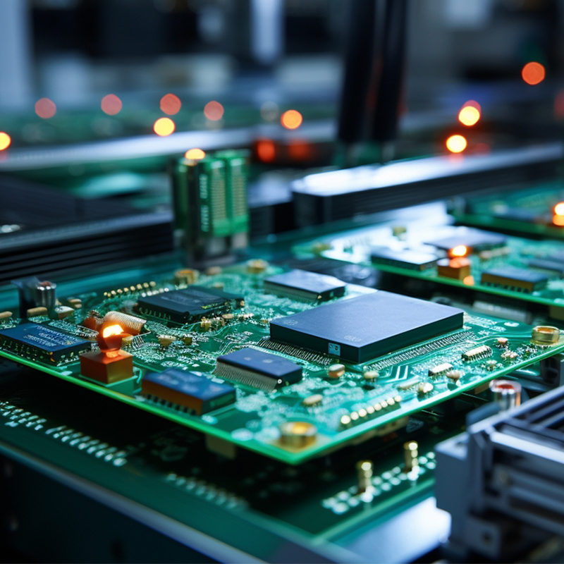
Conductive Ink PCB
Mintec Innovation Technology Industry is an Electronic Manufacturing Service (EMS) provider located in Shenzhen, China, and has been in operation since 2004. Shenzhen, China is the most complete electronic manufacturing base for electronic manufacturing services (EMS) in the world. We provide customers with flexible and reliable electronic manufacturing solutions, one-stop services from logistics,inspections,fabrication,after-sales support,assembly, etc.
The company covers an area of 5,000 square meters and has about 300 employees. Our equipment can meet the needs of many high-precision products. As a supplier with IS09001 quality system certification, we have accumulated rich experience in PCBA assembly and product manufacturing, and implemented strict quality management, which has given us a good reputation in the same industry. Our processing services cover almost every industry, including: IOT,medical,LED lighting,industrial , agriculture and defense, aerospace, etc.

Conductive Ink PCB is one of our PCB products. We will introduce its detailed parameter information and our company advantages to you.
Todos nuestros productos son estrictamente de acuerdo a las regulaciones RoHS / REACH, con precios asequibles con quality.we sin igual cuidar de la calidad de nuestros productos, cualquier defecto de las mercancías, vamos a asumir la responsabilidad. OEM / ODM servicio está disponible.tenemos plena experiencia en la exportación y gestión de proyectos, para asegurar su orden 100%.
| Nombre del producto | Conductive Ink PCB |
| Marca | MTI |
| Lugar de origen | Shenzhen,Guangdong,China |
| Tipo de producto | PCB |
| Certificado | CE,CSA,C-Tick… |
| Garantía | 1 año |
| Puerto | Shenzhen |
| Aplicación | medical,LED lighting...etc. |
| Servicio posventa | Servicio 24 horas |
| Plazo de entrega (días) | 5-15(A negociar) |
Atención: Los datos de la tabla anterior son sólo de referencia. Para información específica, por favor Contacto.
SCHEMATIC DESIGN of Conductive Ink PCB

Capacidades de diseño de MTI ID y MD

This layout shows the exact appearance and placement of the components on Conductive Ink PCB.

