
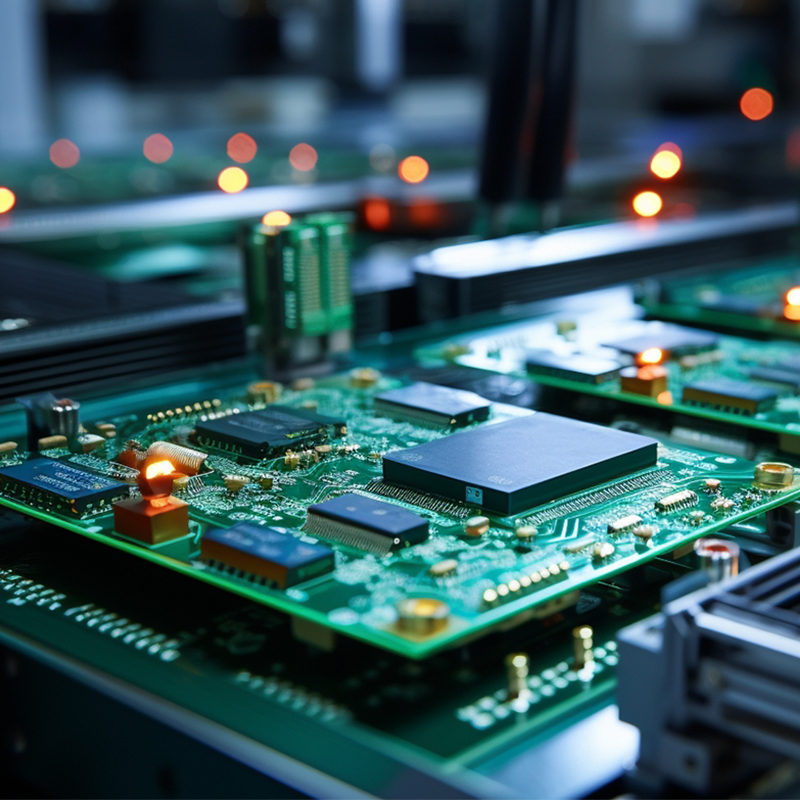
Buried Via PCB
Mintec Innovation Technology Industry Co., Ltd was established in 2004, with 20 years of experience in PCB manufacturing and PCBA assembly, and a professional technical team. PCB and PCBA quality is stable and reliable, with high yield and fast speed. It has sample and mass production workshops, and batch and sample have independent production lines.
The products are suitable for industries including: industrial,LED lighting,telecommunication,IOT, etc. Our factory has advanced equipment such as automatic graphics electroplating production lines,CNC drilling,flying probe tests and automatic test machines,laser exposure machines. And the products have obtained IC,C-Tick,CE,FCC and other certifications. The products are exported to Oceania,Europe,Africa,Asia , and other regions.

Buried Via PCB is one of our PCB products. We will introduce its detailed parameter information and our company advantages to you.
Todos nuestros productos son estrictamente de acuerdo a las regulaciones RoHS / REACH, con precios asequibles con quality.we sin igual cuidar de la calidad de nuestros productos, cualquier defecto de las mercancías, vamos a asumir la responsabilidad. OEM / ODM servicio está disponible.tenemos plena experiencia en la exportación y gestión de proyectos, para asegurar su orden 100%.
| Nombre del producto | Buried Via PCB |
| Palabra clave | circuit card assembly,flexible pcb board,0.5 mm pcb,pcb assembly manufacturer |
| Lugar de origen | China |
| Grosor del tablero | 1~3,2 mm |
| Industrias aplicables | electrónica de consumo, etc. |
| Servicio | Fabricación OEM/ODM |
| Certificado | ISO-9001:2015, ISO-14001:2015,ISO-13485:2012.UL/CSA |
| Color de la máscara de soldadura | Rojo |
| Ventaja | Mantenemos una buena calidad y un precio competitivo para que nuestros clientes se beneficien |
| País de ventas | All over the world for example:Tokelau |
SCHEMATIC DESIGN of Buried Via PCB

Capacidades de diseño de MTI ID y MD

This layout shows the exact appearance and placement of the components on Buried Via PCB.

