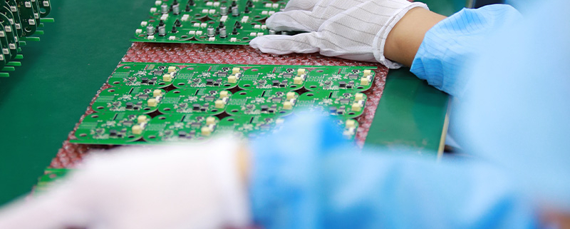
Flex pcba-MTI PCBA
MTI is a manufacturer of high-precision printed circuit board (PCB).We specialize in the manufacture of high precision double-sided and multilayer printed circuit boards, We provide high quality products and faster service for high-tech companies.
We have a group of experienced staff and high-quality management team, set up a complete quality assurance system. Products include FR-4 PCB, Metal PCB and RFPCB (ceramic PCB, PTFE PCB), etc. Have rich experience in the production of thick copper PCB, RF PCB, high Tg PCB, HDI PCB.With ISO9001, ISO14001, TS16949, ISO 13485, RoHS certifications.
| Product name | flex pcba |
| Keyword | eft pcb,12v led pcb,1 oz pcb copper thickness |
| Place of Origin | China |
| Board Thickness | 1~3.2mm |
| Applicable Industries | medical, etc. |
| Service | OEM/ODM manufacturing |
| Certificate | ISO-9001:2015, ISO-14001:2015,ISO-13485:2012.UL/CSA |
| Solder Mask Color | Yellow |
| Advantage | We keep good quality and competitive price to ensure our customers benefit |
| Sales country | All over the world for example:Serbia and Montenegro,Pakistan,Tuvalu,Sierra Leone,Niue,Portugal,Kazakhstan,Thailand,Anguilla |
Your deliverables are always ahead of schedule and of the highest quality.
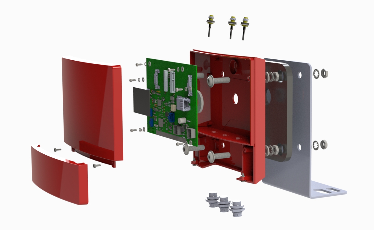
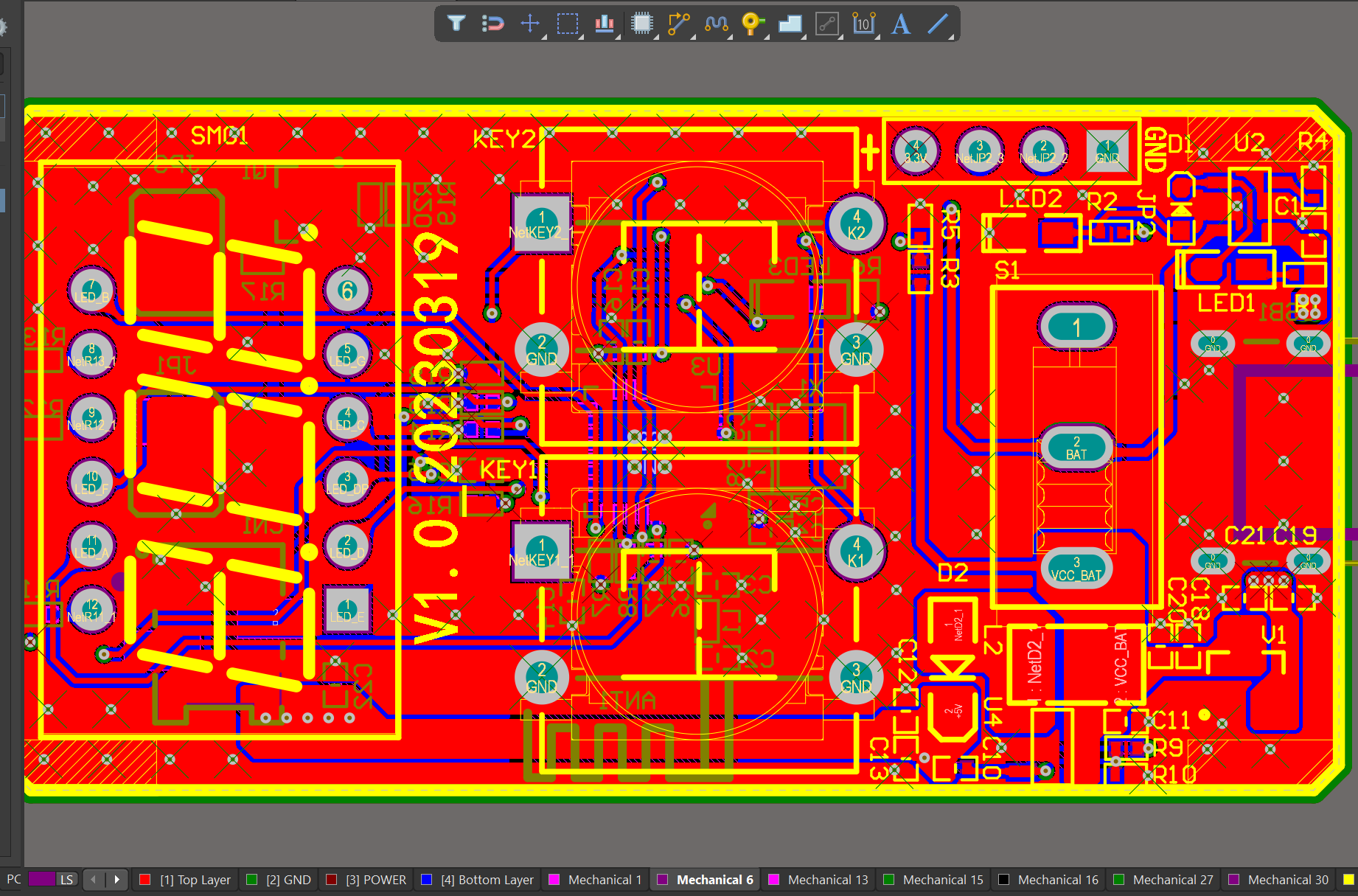
We have rich experience engineer to create a layout using a software platform like Altium Designer. This layout shows you the exact appearance and placement of the components on your board.
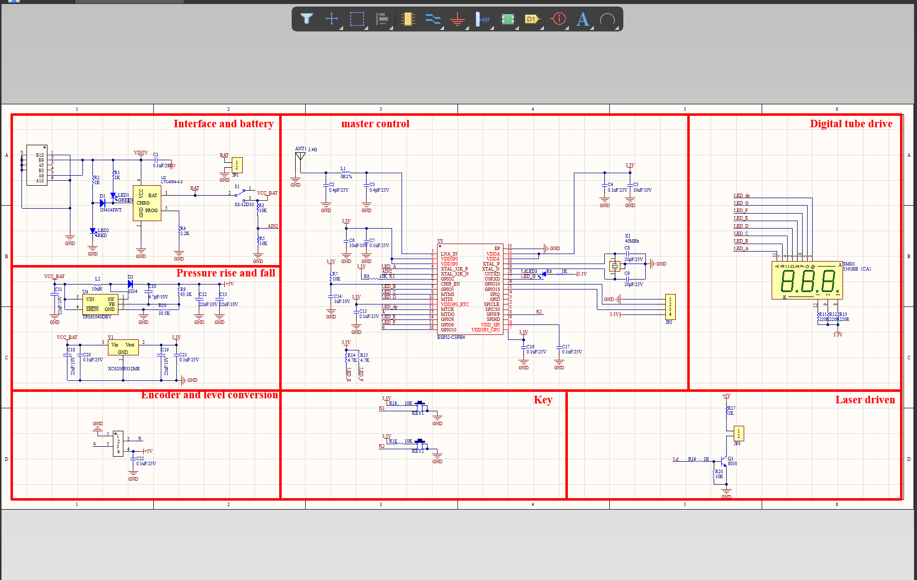
One of our Hardware Design Services is small-batch manufacturing, which allows you to test your idea quickly and verify the functionality of the hardware design and PCB board.
FAQs Guide
2.What are the advantages and disadvantages of using a rigid or flexible PCB?
3.How does the type of PCB finish affect its durability and lifespan?
4.What are the different types of through-hole mounting techniques used in PCBs?
5.What is the difference between single-sided and double-sided PCBs?
1.What are the key features of a PCB?
We are committed to providing personalized solutions and established long -term strategic cooperative relationships with customers.
1. Substrate: The base material on which the circuit is printed, usually made of fiberglass or composite epoxy.
2. Conductive Traces: Thin copper lines that connect the components on the PCB.
3. Pads: Small copper areas on the PCB surface where components are soldered.
4. Vias: Holes drilled through the PCB to connect the different layers of the circuit.
5. Solder Mask: A layer of protective material that covers the copper traces and pads, preventing accidental short circuits.
6. Silkscreen: A layer of ink that is printed on the PCB to label the components and provide other useful information.
7. Components: Electronic devices such as resistors, capacitors, and integrated circuits that are mounted on the PCB.
8. Mounting Holes: Holes drilled on the PCB to allow it to be securely attached to a larger device or enclosure.
9. Copper Pour: Large areas of copper that are used to provide a common ground or power plane for the circuit.
10. Edge Connectors: Metal contacts on the edge of the PCB that allow it to be connected to other circuits or devices.
11. Solder Bridges: Small areas of exposed copper that allow for the connection of two or more traces.
12. Test Points: Small pads or holes on the PCB that allow for testing and troubleshooting of the circuit.
13. Silkscreen Legend: Printed text or symbols on the silkscreen layer that provide additional information about the PCB and its components.
14. Designators: Letters or numbers printed on the silkscreen layer to identify specific components on the PCB.
15. Reference Designators: A combination of letters and numbers that identify the location of a component on the PCB according to the schematic diagram.
2.What are the advantages and disadvantages of using a rigid or flexible PCB?
We have the leading technology and innovation capabilities, and attach importance to employee training and development, and provide promotion opportunities.
Advantages of rigid PCB:
1. Durability: Rigid PCBs are more durable and can withstand higher levels of stress and strain compared to flexible PCBs.
2. Better for high-speed applications: Rigid PCBs are better suited for high-speed applications as they have better signal integrity and lower signal loss.
3. Cost-effective: Rigid PCBs are generally less expensive to manufacture compared to flexible PCBs.
4. Easier to assemble: Rigid PCBs are easier to assemble and can be used with automated assembly processes, making them more efficient for mass production.
5. Higher component density: Rigid PCBs can accommodate a higher number of components and have a higher component density compared to flexible PCBs.
Disadvantages of rigid PCB:
1. Limited flexibility: Rigid PCBs are not flexible and cannot be bent or twisted, making them unsuitable for certain applications.
2. Bulkier: Rigid PCBs are bulkier and take up more space compared to flexible PCBs, which can be a disadvantage in compact electronic devices.
3. Prone to damage: Rigid PCBs are more prone to damage from vibrations and shocks, which can affect their performance.
Advantages of flexible PCB:
1. Flexibility: Flexible PCBs can be bent, twisted, and folded, making them suitable for applications where space is limited or where the PCB needs to conform to a specific shape.
2. Lightweight: Flexible PCBs are lightweight and take up less space compared to rigid PCBs, making them ideal for portable electronic devices.
3. Better for high vibration environments: Flexible PCBs are more resistant to vibrations and shocks, making them suitable for use in high vibration environments.
4. Higher reliability: Flexible PCBs have fewer interconnects and solder joints, reducing the chances of failure and increasing reliability.
Disadvantages of flexible PCB:
1. Higher cost: Flexible PCBs are generally more expensive to manufacture compared to rigid PCBs.
2. Limited component density: Flexible PCBs have a lower component density compared to rigid PCBs, which can limit their use in high-density applications.
3. Difficult to repair: Flexible PCBs are more difficult to repair compared to rigid PCBs, as they require specialized equipment and expertise.
4. Less suitable for high-speed applications: Flexible PCBs have higher signal loss and lower signal integrity compared to rigid PCBs, making them less suitable for high-speed applications.
3.How does the type of PCB finish affect its durability and lifespan?
I have a comprehensive after -sales service system, which can pay attention to market trends in time and adjust our strategy in a timely manner.
The type of PCB finish can have a significant impact on the durability and lifespan of a PCB. The finish is the final coating applied to the surface of the PCB to protect it from environmental factors and ensure proper functionality. Some common types of PCB finishes include HASL (Hot Air Solder Leveling), ENIG (Electroless Nickel Immersion Gold), and OSP (Organic Solderability Preservative).
1. HASL (Hot Air Solder Leveling):
HASL is a popular and cost-effective finish that involves coating the PCB with a layer of molten solder and then leveling it with hot air. This finish provides good solderability and is suitable for most applications. However, it is not very durable and can be prone to oxidation, which can affect the performance of the PCB over time. HASL finish also has a limited shelf life and may require rework after a certain period.
2. ENIG (Electroless Nickel Immersion Gold):
ENIG is a more advanced and durable finish compared to HASL. It involves depositing a layer of nickel and then a layer of gold on the surface of the PCB. This finish provides excellent corrosion resistance and is suitable for high-reliability applications. ENIG finish also has a longer shelf life and does not require rework as frequently as HASL.
3. OSP (Organic Solderability Preservative):
OSP is a thin organic coating applied to the surface of the PCB to protect it from oxidation. It is a cost-effective finish and provides good solderability. However, OSP finish is not as durable as ENIG and may require rework after a certain period. It is also not suitable for high-temperature applications.
In summary, the type of PCB finish can affect its durability and lifespan in the following ways:
– Corrosion resistance: Finishes like ENIG and OSP provide better corrosion resistance compared to HASL, which can affect the performance and lifespan of the PCB.
– Shelf life: Finishes like ENIG have a longer shelf life compared to HASL, which may require rework after a certain period.
– Solderability: All finishes provide good solderability, but ENIG and OSP are more suitable for high-reliability applications.
– Environmental factors: The type of finish can also affect the PCB’s resistance to environmental factors like humidity, temperature, and chemicals, which can impact its durability and lifespan.
In conclusion, choosing the right type of PCB finish is crucial for ensuring the durability and longevity of the PCB. Factors such as the application, environmental conditions, and budget should be considered when selecting the appropriate finish for a PCB.
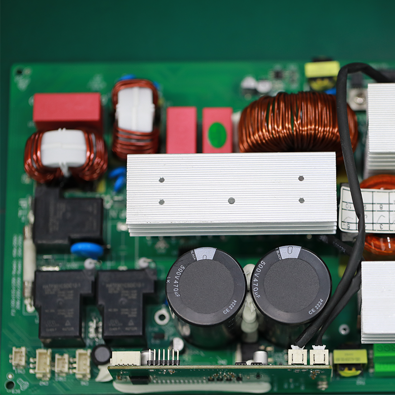
4.What are the different types of through-hole mounting techniques used in PCBs?
We have flexible production capacity. Whether you are large orders or small orders, you can produce and release goods in a timely manner to meet customer needs.
1. Through-Hole Plating: This is the most common through-hole mounting technique, where the holes in the PCB are plated with a conductive material, usually copper, to create a connection between the layers of the board.
2. Through-Hole Soldering: In this technique, the components are inserted into the plated holes and then soldered to the pads on the opposite side of the board. This provides a strong mechanical connection and good electrical conductivity.
3. Through-Hole Riveting: In this method, the components are inserted into the plated holes and then secured with a rivet or pin. This is commonly used for high-power components or in applications where the board may experience high levels of vibration.
4. Through-Hole Press-Fit: This technique involves inserting the component leads into the plated holes and then pressing them into place using a specialized tool. This provides a strong mechanical connection without the need for soldering.
5. Through-Hole Wave Soldering: In this method, the components are inserted into the plated holes and then passed over a wave of molten solder, which creates a strong solder joint between the component leads and the PCB pads.
6. Through-Hole Reflow Soldering: This technique is similar to wave soldering, but instead of passing over a wave of molten solder, the board is heated in a controlled environment to melt the solder and create a strong joint.
7. Through-Hole Hand Soldering: This is a manual method of soldering where the components are inserted into the plated holes and then soldered by hand using a soldering iron. This is commonly used for small-scale production or for repairs.
8. Through-Hole Pin-in-Paste: This technique involves inserting the component leads into the plated holes and then applying solder paste to the holes before reflow soldering. This provides a strong mechanical connection and good solder joints.
9. Through-Hole Pin-in-Hole: In this method, the component leads are inserted into the plated holes and then bent to form a right angle, creating a secure mechanical connection. This is commonly used for components with large leads, such as electrolytic capacitors.
10. Through-Hole Hand Assembly: This is a manual method of assembly where the components are inserted into the plated holes and then secured with hand tools, such as screws or nuts. This is commonly used for large or heavy components that require additional support.
5.What is the difference between single-sided and double-sided PCBs?
Our mission is to provide customers with the best solutions for flex pcba.
Single-sided PCBs have copper traces and components on only one side of the board, while double-sided PCBs have copper traces and components on both sides of the board. This allows for more complex circuit designs and a higher density of components on a double-sided PCB. Single-sided PCBs are typically used for simpler circuits and are less expensive to manufacture, while double-sided PCBs are used for more complex circuits and are more expensive to manufacture.
Tags:108 keyboard pcb,pcb boards,h60 pcb
