MTI Developed 5G CPE from Schematic Design to PCB Assembly
Empowering Connectivity: The Evolution of 5G CPE Technology
5G CPE, or 5G Customer Premise Equipment, is a device that connects to a 5G network and provides internet access to other devices via Wi-Fi or Ethernet. 5G CPE can offer faster and more reliable internet service than traditional routers or modems, as it can support higher bandwidth, lower latency, and wider coverage. In this article, we will share our development experience for 5G CPE, from schematic design to PCB assembly.
Schematic Design
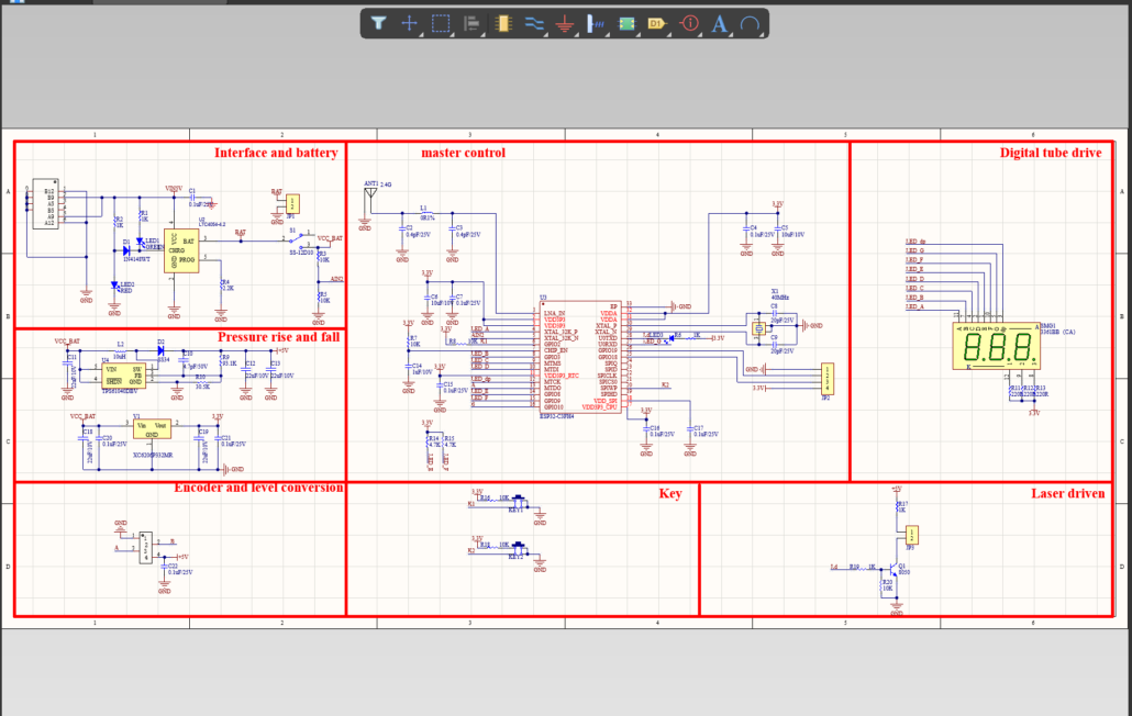
The first step of our development process was to design the schematic of the 5G CPE device. The schematic is a graphical representation of the electrical connections and components of the device. The schematic shows how the power supply, the 5G module, the Wi-Fi module, the Ethernet module, the antenna, and other parts are connected and configured. The schematic also specifies the values and ratings of the resistors, capacitors, inductors, diodes, transistors, and other components.
To design the schematic, we used [EAGLE], a software tool that allows us to create and edit schematic diagrams easily and efficiently. EAGLE has a library of thousands of standard components that we can drag and drop into our schematic. EAGLE also has a simulation feature that allows us to test and verify our schematic before moving on to the next step.

PCB Layout
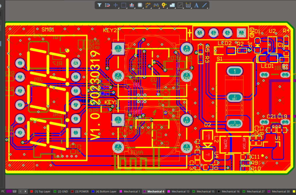
The second step of our development process was to design the PCB layout of the 5G CPE device. The PCB layout is a physical representation of the arrangement and placement of the components and traces on the printed circuit board. The PCB layout shows how the components are mounted on the board, how the traces are routed between them, and how the board is shaped and sized.
To design the PCB layout, we used [KiCad], a software tool that allows us to create and edit PCB layouts easily and efficiently. KiCad has a feature that allows us to import our schematic from EAGLE and automatically generate a PCB layout based on it. KiCad also has a 3D viewer that allows us to see how our PCB layout looks like in real life.

PCB Assembly
The third and final step of our development process was to assemble the PCB of the 5G CPE device. The PCB assembly is the process of soldering the components onto the printed circuit board according to the PCB layout. The PCB assembly requires precision and accuracy, as any mistake or defect can affect the performance or functionality of the device.
To assemble the PCB, we used [JLCPCB], a professional PCB manufacturer that offers high-quality PCB assembly services at low prices. JLCPCB has a feature that allows us to upload our PCB layout file and order our PCBs online. JLCPCB also has a large inventory of standard components that we can choose from for our PCB assembly. JLCPCB can deliver our assembled PCBs within a few days.
We have successfully developed 5G CPE from schematic design to PCB assembly using various software tools and services. We have learned a lot from this project, and we are proud of our achievement. We hope that our development experience can inspire and help others who are interested in creating their own 5G CPE devices. If you have any questions or feedback, please feel free to contact us. Thank you for reading.


