
Understanding the PCBA (Printed Circuit Board Assembly) Process
Understanding the PCBA (Printed Circuit Board Assembly) Process
Introduction:
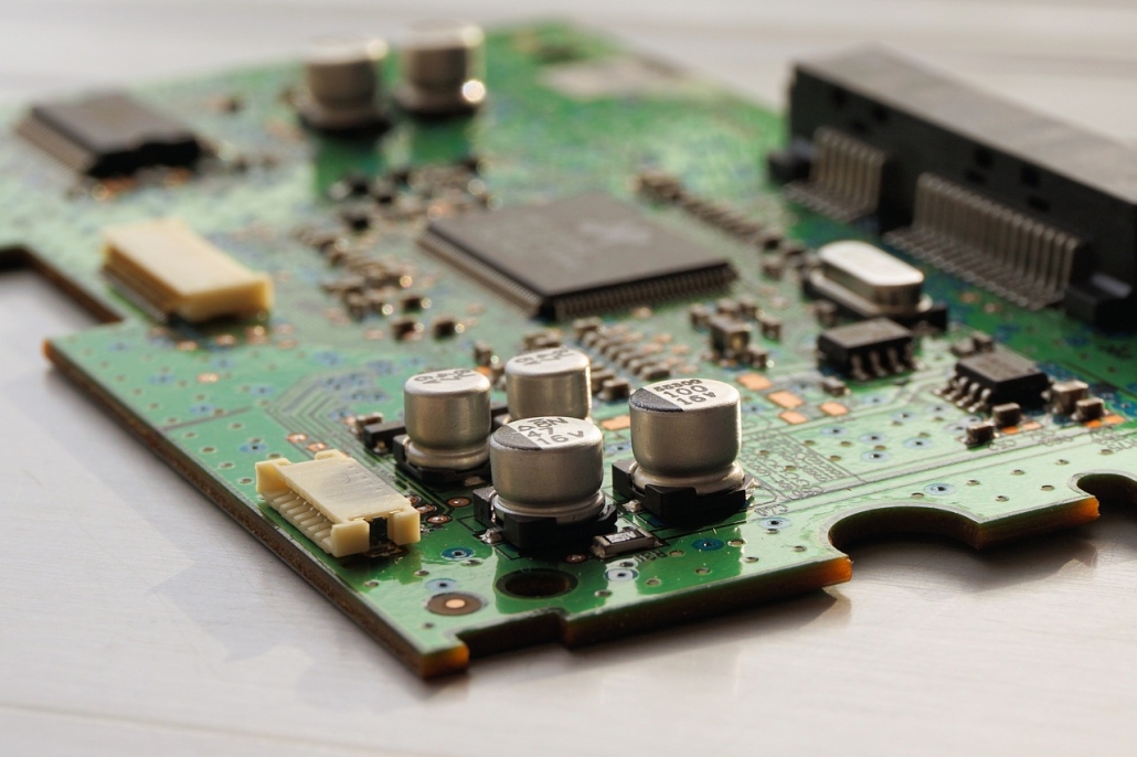
PCBA, which stands for Printed Circuit Board Assembly, is a crucial step in the manufacturing of electronic devices. It involves attaching electronic components to a printed circuit board (PCB) to create a functional electronic circuit. This intricate process forms the backbone of modern electronics manufacturing, and here, we delve into the various stages involved.
PCBA Process:
Solder Paste Stenciling:
After the bare PCB is fabricated, solder paste is applied to the pads for Surface Mount Technology (SMT).
Solder paste, composed of tin, silver, and copper, facilitates physical and electrical connections between components and the board.
A precise machine applies solder paste evenly, guided by a stencil tailored to the PCB layout.
Pick and Place:
A robotic pick-and-place machine rapidly positions Surface Mount Devices (SMDs) on the PCB.
These machines are programmed for specific projects, ensuring accurate component placement.
As components shrink in size, specialized machines handle the tiniest SMDs.
Reflow Soldering:
Once components and solder paste are in place, the PCB undergoes reflow soldering.
The board is heated in stages to 250°C, melting the solder paste and solidifying it as it cools.
This controlled process ensures secure component attachment.
Inspection and Quality Control:
After SMT, a thorough inspection checks physical and electrical connections.
Automatic Optical Inspection (AOI) machines use cameras to identify solder joint quality.
Defective boards are reworked or discarded based on quality standards.
Through-Hole Component Insertion:
Plated Through-Holes (PTH) are utilized when necessary for components.
These holes enable signals to pass through the board.
Workers manually insert PTH components into the board.
Wave Soldering:
Wave soldering is employed for mass production, eliminating hand soldering.
Boards move through a wave solder machine, where a molten solder wave solders the PTH components’ joints.
Care must be taken with double-sided PCBs to prevent damage.
Final Inspection and Functional Test:
The PCB undergoes a functional test simulating real-world conditions.
Electrical characteristics, such as voltage, current, and signal output, are examined.
Any deviations from predetermined ranges indicate a failed PCB.
Cleaning:
After assembly, residual solder paste, oils, and contaminants are removed.
High-pressure washing with deionized water ensures a clean board.
The PCB is dried and prepared for packaging.
The PCBA process is the backbone of electronic manufacturing, ensuring the creation of reliable and functional electronic devices. Each stage, from soldering to testing, plays a vital role in producing high-quality PCBAs that power our modern world. Understanding this process sheds light on the complexity and precision required in electronics manufacturing.

