1 layer pcb
MTI is a high-tech company specializing in PCB manufacturing, PCB assembly and parts procurement services with more than 20 years of experience. We are committed to producing various types of printed circuit boards, mainly including single-sided, double-sided, multi-layer circuit boards, high-precision HDI, flexible boards (FPC), rigid-flex boards (including HDI), metal circuit boards and their SMD plugin.Product line application areas include:aerospace.Fast response, strict quality control, best service, and strong technical support export our PCB products to global markets,including,France,Liberia,Turkmenistan,Tunisia,Syria,El Salvador,Cambodia,Tuvalu,Finland.
MTI would like to build long and stable business relationship with the customers from all over the world on the basis of mutual benefits and mutual progress;Choose MTI , Drive you Success!
| Product name | 1 layer pcb |
| Keyword | pcb fabrication and assembly,printed circuit board assembly process |
| Place of Origin | China |
| Board Thickness | 1~3.2mm |
| Applicable Industries | medical equipment, etc. |
| Service | OEM/ODM manufacturing |
| Certificate | ISO-9001:2015, ISO-14001:2015,ISO-13485:2012.UL/CSA |
| Solder Mask Color | Red |
| Advantage | We keep good quality and competitive price to ensure our customers benefit |
| Sales country | All over the world for example:France,Liberia,Turkmenistan,Tunisia,Syria,El Salvador,Cambodia,Tuvalu,Finland |
Your deliverables are always ahead of schedule and of the highest quality.

One of our Hardware Design Services is small-batch manufacturing, which allows you to test your idea quickly and verify the functionality of the hardware design and PCB board.

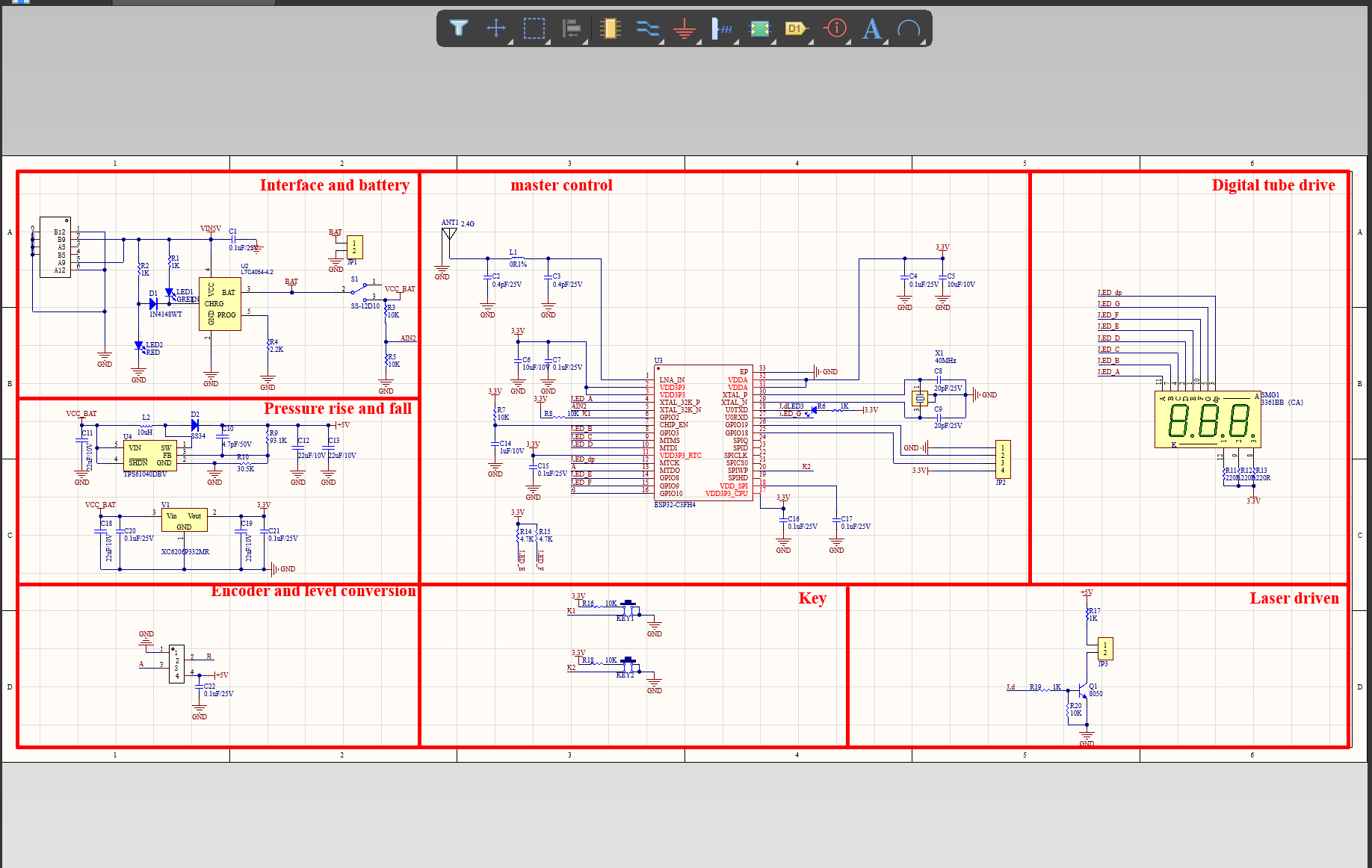
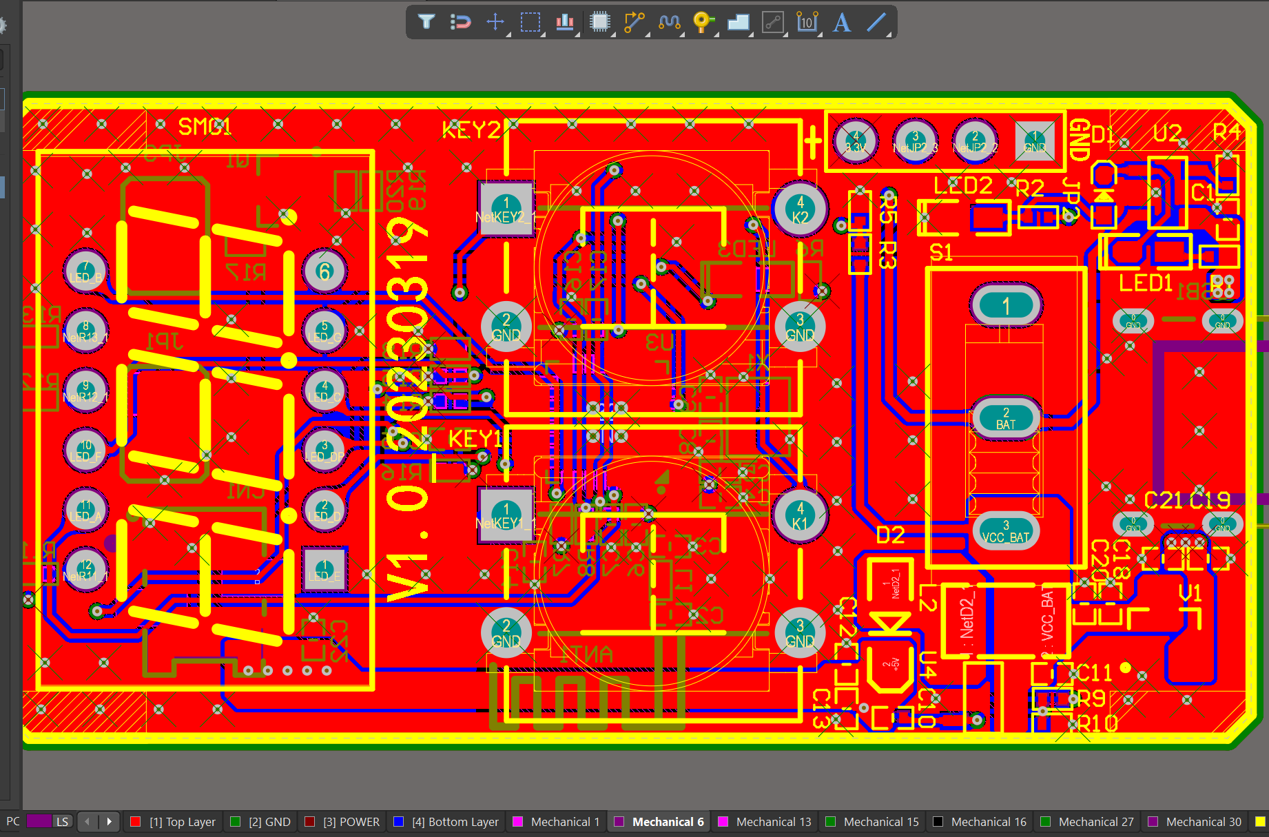
We have rich experience engineer to create a layout using a software platform like Altium Designer. This layout shows you the exact appearance and placement of the components on your board.

FAQs Guide
2.Can PCBs have different shapes and sizes?
3.What is thermal management in PCBs and why is it important?
4.Can PCBs be designed with high-speed and high-frequency applications in mind?
5.Can PCBs be made with different thicknesses?
6.How does the type of PCB finish affect its durability and lifespan?
1.How does component placement affect signal integrity in a PCB design?
We pay attention to the transformation of intellectual property protection and innovation achievements. Your OEM or ODM order design we have a complete confidentiality system.
Component placement plays a crucial role in determining the signal integrity of a PCB design. The placement of components affects the routing of traces, which in turn affects the impedance, crosstalk, and signal integrity of the 1 layer PCB.
1. Impedance: The placement of components affects the impedance of the traces. If components are placed too far apart, the traces will be longer, resulting in higher impedance. This can lead to signal reflections and degradation of the signal.
2. Crosstalk: Crosstalk is the interference between two traces on a PCB. The placement of components can affect the distance between traces, which can increase or decrease crosstalk. If components are placed too close together, the crosstalk between traces can increase, leading to signal distortion.
3. Signal routing: The placement of components also affects the routing of traces. If components are placed in a way that requires traces to make sharp turns or cross over each other, it can result in signal degradation. This can be avoided by carefully placing components in a way that allows for smooth and direct routing of traces.
4. Grounding: Proper grounding is essential for maintaining signal integrity. The placement of components can affect the grounding scheme of the PCB. If components are placed too far from the ground plane, it can result in a longer return path for signals, leading to ground bounce and noise.
5. Thermal considerations: The placement of components can also affect the thermal performance of the PCB. If components that generate a lot of heat are placed too close together, it can result in hot spots and affect the performance of the PCB.
To ensure good signal integrity, it is important to carefully consider the placement of components during the PCB design process. Components should be placed in a way that minimizes trace length, reduces crosstalk, allows for direct routing of traces, and ensures proper grounding and thermal management.
2.Can PCBs have different shapes and sizes?
Our company has many years of 1 layer pcb experience and expertise.
Yes, PCBs (printed circuit boards) can have different shapes and sizes depending on the specific design and purpose of the circuit. They can range from small and compact to large and complex, and can be rectangular, circular, or even irregularly shaped. The shape and size of a PCB is determined by the layout of the components and the desired functionality of the circuit.
3.What is thermal management in PCBs and why is it important?
We have been working hard to improve service quality and meet customer needs.
Thermal management in PCBs (Printed Circuit Boards) refers to the techniques and strategies used to control and dissipate heat generated by electronic components on the board. It is important because excessive heat can damage components, reduce their performance, and even cause the PCB to fail. Proper thermal management is crucial for ensuring the reliability and longevity of electronic devices.
The electronic components on a PCB generate heat due to the flow of electricity through them. This heat can build up and cause the temperature of the 1 layer PCB to rise, potentially leading to malfunctions or failures. Thermal management techniques are used to dissipate this heat and maintain the temperature of the PCB within safe operating limits.
There are several methods of thermal management in PCBs, including heat sinks, thermal vias, and thermal pads. Heat sinks are metal components attached to hot components on the PCB to absorb and dissipate heat. Thermal vias are small holes drilled into the PCB to allow heat to escape to the other side of the board. Thermal pads are used to transfer heat from components to the PCB and then to the surrounding air.
Proper thermal management is especially important in high-power and high-density PCBs, where heat generation is more significant. It is also crucial in applications where the PCB is exposed to extreme temperatures or harsh environments. Without effective thermal management, the performance and reliability of electronic devices can be compromised, leading to costly repairs or replacements.
4.Can PCBs be designed with high-speed and high-frequency applications in mind?
We attach importance to the innovation ability and team spirit of employees, have advanced R & D facilities and laboratories, and have a good quality management system.
Yes, PCBs can be designed with high-speed and high-frequency applications in mind. This involves careful consideration of the layout, trace routing, and component placement to minimize signal loss and interference. Specialized materials and techniques, such as controlled impedance routing and differential pairs, can also be used to improve signal integrity and reduce noise. Additionally, the use of advanced simulation and analysis tools can help optimize the design for high-speed and high-frequency performance.

5.Can PCBs be made with different thicknesses?
We operate our 1 layer pcb business with integrity and honesty.
Yes, PCBs (printed circuit boards) can be made with different thicknesses. The thickness of a PCB is determined by the thickness of the copper layer and the thickness of the substrate material. The copper layer thickness can range from 0.5 oz to 3 oz, while the substrate material thickness can range from 0.2 mm to 3.2 mm. The most common thicknesses for PCBs are 1.6 mm and 0.8 mm, but custom thicknesses can be requested from PCB manufacturers. The thickness of a PCB can affect its mechanical strength, thermal properties, and electrical performance.
6.How does the type of PCB finish affect its durability and lifespan?
I have a comprehensive after -sales service system, which can pay attention to market trends in time and adjust our strategy in a timely manner.
The type of PCB finish can have a significant impact on the durability and lifespan of a 1 layer PCB. The finish is the final coating applied to the surface of the PCB to protect it from environmental factors and ensure proper functionality. Some common types of PCB finishes include HASL (Hot Air Solder Leveling), ENIG (Electroless Nickel Immersion Gold), and OSP (Organic Solderability Preservative).
1. HASL (Hot Air Solder Leveling):
HASL is a popular and cost-effective finish that involves coating the PCB with a layer of molten solder and then leveling it with hot air. This finish provides good solderability and is suitable for most applications. However, it is not very durable and can be prone to oxidation, which can affect the performance of the PCB over time. HASL finish also has a limited shelf life and may require rework after a certain period.
2. ENIG (Electroless Nickel Immersion Gold):
ENIG is a more advanced and durable finish compared to HASL. It involves depositing a layer of nickel and then a layer of gold on the surface of the PCB. This finish provides excellent corrosion resistance and is suitable for high-reliability applications. ENIG finish also has a longer shelf life and does not require rework as frequently as HASL.
3. OSP (Organic Solderability Preservative):
OSP is a thin organic coating applied to the surface of the PCB to protect it from oxidation. It is a cost-effective finish and provides good solderability. However, OSP finish is not as durable as ENIG and may require rework after a certain period. It is also not suitable for high-temperature applications.
In summary, the type of PCB finish can affect its durability and lifespan in the following ways:
– Corrosion resistance: Finishes like ENIG and OSP provide better corrosion resistance compared to HASL, which can affect the performance and lifespan of the PCB.
– Shelf life: Finishes like ENIG have a longer shelf life compared to HASL, which may require rework after a certain period.
– Solderability: All finishes provide good solderability, but ENIG and OSP are more suitable for high-reliability applications.
– Environmental factors: The type of finish can also affect the PCB’s resistance to environmental factors like humidity, temperature, and chemicals, which can impact its durability and lifespan.
In conclusion, choosing the right type of PCB finish is crucial for ensuring the durability and longevity of the PCB. Factors such as the application, environmental conditions, and budget should be considered when selecting the appropriate finish for a PCB.
Tags:1000 watt amplifier pcb,2.4 ghz yagi pcb antenna
