
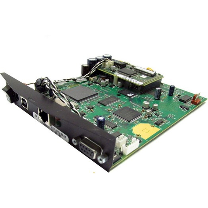
12 layer pcb thickness
MTI is a high-tech company specializing in PCB manufacturing, PCB assembly and parts procurement services with more than 20 years of experience. We are committed to producing various types of printed circuit boards, mainly including single-sided, double-sided, multi-layer circuit boards, high-precision HDI, flexible boards (FPC), rigid-flex boards (including HDI), metal circuit boards and their SMD plugin.Product line application areas include:testing instruments.Fast response, strict quality control, best service, and strong technical support export our PCB products to global markets,including,Philippines,Anguilla,Chad,Peru,Burundi,Togo,Martinique,Zimbabwe,Mali.
MTI would like to build long and stable business relationship with the customers from all over the world on the basis of mutual benefits and mutual progress;Choose MTI , Drive you Success!
| Product name | 12 layer pcb thickness |
| Keyword | 1073 pcb,16 layer pcb manufacturer,12v battery charger pcb |
| Place of Origin | China |
| Board Thickness | 1~3.2mm |
| Applicable Industries | automotive electronics , etc. |
| Service | OEM/ODM manufacturing |
| Certificate | ISO-9001:2015, ISO-14001:2015,ISO-13485:2012.UL/CSA |
| Solder Mask Color | Yellow |
| Advantage | We keep good quality and competitive price to ensure our customers benefit |
| Sales country | All over the world for example:Philippines,Anguilla,Chad,Peru,Burundi,Togo,Martinique,Zimbabwe,Mali |
One of our Hardware Design Services is small-batch manufacturing, which allows you to test your idea quickly and verify the functionality of the hardware design and PCB board.

We have rich experience engineer to create a layout using a software platform like Altium Designer. This layout shows you the exact appearance and placement of the components on your board.

Your deliverables are always ahead of schedule and of the highest quality.

FAQs Guide
2.How does the type of vias used affect the performance of a PCB?
3.What is testability in PCB design and how is it achieved?
4.How does the type of solder mask used affect the PCB’s performance?
5.Can a PCB have different levels of flexibility?
1.How do PCBs handle overcurrent and short circuits?
We have a first -class management team, and we pay attention to teamwork to achieve common goals.
PCBs (printed circuit boards) have several mechanisms in place to handle overcurrent and short circuits:
1. Fuses: Fuses are the most common protection mechanism used on PCBs. They are designed to break the circuit when the current exceeds a certain threshold, preventing damage to the components and the board.
2. Circuit breakers: Similar to fuses, circuit breakers are designed to break the circuit when the current exceeds a certain threshold. However, unlike fuses, circuit breakers can be reset and reused.
3. Overcurrent protection devices: These devices, such as overcurrent protection diodes, are designed to limit the amount of current flowing through the circuit. They act as a safety valve, preventing excessive current from damaging the components.
4. Thermal protection: Some PCBs have thermal protection mechanisms, such as thermal fuses or thermal cutoffs, which are designed to break the circuit when the temperature of the board exceeds a certain threshold. This helps prevent damage to the board and components due to overheating.
5. Short circuit protection: PCBs may also have short circuit protection mechanisms, such as polymeric positive temperature coefficient (PPTC) devices, which are designed to limit the current in the event of a short circuit. These devices have a high resistance at normal operating temperatures, but their resistance increases significantly when the temperature rises due to a short circuit, limiting the current flow.
Overall, PCBs use a combination of these protection mechanisms to handle overcurrent and short circuits, ensuring the safety and reliability of the board and its components.
2.How does the type of vias used affect the performance of a PCB?
Being one of the top 12 layer pcb thickness manufacturers in China, We attach great importance to this detail.
The type of vias used can affect the performance of a PCB in several ways:
1. Signal Integrity: Vias can act as discontinuities in the signal path, causing reflections and signal degradation. The type of via used can impact the impedance and signal integrity of the PCB. For high-speed signals, it is important to use controlled impedance vias to maintain signal integrity.
2. Electrical Performance: The type of via used can also affect the electrical performance of the PCB. For example, through-hole vias have lower resistance and inductance compared to blind or buried vias, which can affect the power delivery and signal transmission on the PCB.
3. Thermal Performance: Vias can also play a role in the thermal performance of a PCB. Through-hole vias can act as thermal vias, allowing heat to dissipate from one layer to another. Blind and buried vias, on the other hand, can trap heat and affect the overall thermal management of the PCB.
4. Manufacturing Cost: The type of via used can also impact the cost of manufacturing the PCB. Blind and buried vias require more complex and expensive processes, while through-hole vias are relatively simpler and cheaper to manufacture.
5. PCB Size and Density: The type of via used can also affect the size and density of the PCB. Blind and buried vias take up less space on the surface of the PCB, allowing for higher density designs. This can be beneficial for smaller and more compact PCBs.
Overall, the type of vias used can have a significant impact on the performance, cost, and design of a PCB. It is important to carefully consider the type of vias needed for a specific application to ensure optimal performance and functionality of the PCB.
3.What is testability in PCB design and how is it achieved?
Our 12 layer pcb thickness products undergo strict quality control to ensure customer satisfaction.
Testability in PCB design refers to the ease and accuracy with which a printed circuit board (PCB) can be tested for functionality and performance. It is an important aspect of PCB design as it ensures that any defects or issues with the board can be identified and addressed before it is put into use.
Achieving testability in PCB design involves implementing certain design features and techniques that make it easier to test the board. These include:
1. Design for Test (DFT): This involves designing the PCB with specific test points and access points that allow for easy and accurate testing of different components and circuits.
2. Test Points: These are designated points on the PCB where test probes can be connected to measure voltage, current, and other parameters. Test points should be strategically placed to provide access to critical components and circuits.
3. Test Pads: These are small copper pads on the PCB that are used for attaching test probes. They should be placed close to the corresponding component or circuit for accurate testing.
4. Test Jigs: These are specialized tools used for testing PCBs. They can be custom-made for a specific PCB design and can greatly improve the accuracy and efficiency of testing.
5. Design for Manufacturability (DFM): This involves designing the PCB with manufacturing and testing in mind. This includes using standard components, avoiding complex layouts, and minimizing the number of layers to make testing easier.
6. Design for Debug (DFD): This involves designing the PCB with features that make it easier to identify and troubleshoot any issues that may arise during testing.
Overall, achieving testability in PCB design requires careful planning and consideration of the testing process. By implementing DFT, using test points and pads, and designing for manufacturability and debug, designers can ensure that their PCBs are easily testable and can be quickly and accurately diagnosed for any potential issues.
4.How does the type of solder mask used affect the PCB’s performance?
We have broad development space in domestic and foreign markets. 12 layer pcb thicknesss have great advantages in terms of price, quality, and delivery date.
The type of solder mask used can affect the PCB’s performance in several ways:
1. Insulation: Solder mask is used to insulate the copper traces on a PCB, preventing them from coming into contact with each other and causing a short circuit. The type of solder mask used can affect the level of insulation provided, which can impact the overall reliability and functionality of the PCB.
2. Solderability: Solder mask also plays a crucial role in the soldering process. The type of solder mask used can affect the surface tension and wetting properties of the solder, which can impact the quality of the solder joints and the overall reliability of the PCB.
3. Thermal resistance: Solder mask can also act as a thermal barrier, protecting the PCB from excessive heat. The type of solder mask used can affect the thermal resistance of the PCB, which can impact its ability to dissipate heat and its overall thermal performance.
4. Chemical resistance: Solder mask is also exposed to various chemicals during the PCB manufacturing process, such as flux and cleaning agents. The type of solder mask used can affect its resistance to these chemicals, which can impact the overall durability and reliability of the PCB.
5. Electrical properties: The type of solder mask used can also affect the electrical properties of the PCB, such as its dielectric constant and dissipation factor. These properties can impact the performance of high-frequency circuits and signal integrity.
Overall, the type of solder mask used can have a significant impact on the performance, reliability, and durability of a PCB. It is essential to carefully select the appropriate solder mask for a specific application to ensure optimal performance.

5.Can a PCB have different levels of flexibility?
We have a wide range of 12 layer pcb thickness customer groups and establishes long -term cooperative relationships with partners.
Yes, a PCB (printed circuit board) can have different levels of flexibility depending on its design and materials used. Some PCBs are rigid and cannot bend or flex at all, while others are designed to be flexible and can bend or twist to a certain degree. There are also PCBs that have a combination of rigid and flexible areas, known as flex-rigid PCBs. The level of flexibility in a PCB is determined by factors such as the type of substrate material, the thickness and number of layers, and the type of circuit design.
Tags:pcb assembly and manufacturing,prototype circuit board assembly,flex pcba manufacturer

