
pcb assembly and manufacturing
MTI specializes in turn-key electronics pcb assembly and manufacturing service, providing comprehensive solutions from product documentation to high-quality product delivery worldwide.
With a wide range, good quality, reasonable prices and stylish designs, our products are extensively used in medical.Our products are widely recognized and trusted by users and can meet continuously changing economic and social needs.We welcome new and old customers from all walks of life to contact us for future business relationships and mutual success!
| Product name | pcb assembly and manufacturing |
| Keyword | prototype printed circuit board assembly,10 oz copper pcb,pcb production and assembly,pcb manufacturers,108 keyboard pcb |
| Place of Origin | China |
| Board Thickness | 2~3.2mm |
| Applicable Industries | security, etc. |
| Service | OEM/ODM manufacturing |
| Certificate | ISO-9001:2015, ISO-14001:2015,ISO-13485:2012.UL/CSA |
| Solder Mask Color | Red |
| Advantage | We keep good quality and competitive price to ensure our customers benefit |
| Sales country | All over the world for example:Argentina,Lithuania,Seychelles,Indonesia,Ireland,Gibraltar |
One of our Hardware Design Services is small-batch manufacturing, which allows you to test your idea quickly and verify the functionality of the hardware design and PCB board.

Your deliverables are always ahead of schedule and of the highest quality.

We have rich experience engineer to create a layout using a software platform like Altium Designer. This layout shows you the exact appearance and placement of the components on your board.

FAQs Guide
2.What is thermal management in PCBs and why is it important?
3.Can PCBs have multiple power planes?
4.How do PCBs handle overcurrent and short circuits?
5.How does the type of solder mask used affect the PCB’s performance?
1.What are the key features of a PCB?
We are committed to providing personalized solutions and established long -term strategic cooperative relationships with customers.
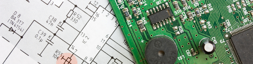
1. Substrate: The base material on which the circuit is printed, usually made of fiberglass or composite epoxy.
2. Conductive Traces: Thin copper lines that connect the components on the PCB.
3. Pads: Small copper areas on the PCB surface where components are soldered.
4. Vias: Holes drilled through the PCB to connect the different layers of the circuit.
5. Solder Mask: A layer of protective material that covers the copper traces and pads, preventing accidental short circuits.
6. Silkscreen: A layer of ink that is printed on the PCB to label the components and provide other useful information.
7. Components: Electronic devices such as resistors, capacitors, and integrated circuits that are mounted on the PCB.
8. Mounting Holes: Holes drilled on the PCB to allow it to be securely attached to a larger device or enclosure.
9. Copper Pour: Large areas of copper that are used to provide a common ground or power plane for the circuit.
10. Edge Connectors: Metal contacts on the edge of the PCB that allow it to be connected to other circuits or devices.
11. Solder Bridges: Small areas of exposed copper that allow for the connection of two or more traces.
12. Test Points: Small pads or holes on the PCB that allow for testing and troubleshooting of the circuit.
13. Silkscreen Legend: Printed text or symbols on the silkscreen layer that provide additional information about the PCB and its components.
14. Designators: Letters or numbers printed on the silkscreen layer to identify specific components on the PCB.
15. Reference Designators: A combination of letters and numbers that identify the location of a component on the PCB according to the schematic diagram.
2.What is thermal management in PCBs and why is it important?
We have been working hard to improve service quality and meet customer needs.
Thermal management in PCBs (Printed Circuit Boards) refers to the techniques and strategies used to control and dissipate heat generated by electronic components on the board. It is important because excessive heat can damage components, reduce their performance, and even cause the PCB to fail. Proper thermal management is crucial for ensuring the reliability and longevity of electronic devices.
The electronic components on a PCB generate heat due to the flow of electricity through them. This heat can build up and cause the temperature of the PCB to rise, potentially leading to malfunctions or failures. Thermal management techniques are used to dissipate this heat and maintain the temperature of the PCB within safe operating limits.
There are several methods of thermal management in PCBs, including heat sinks, thermal vias, and thermal pads. Heat sinks are metal components attached to hot components on the PCB to absorb and dissipate heat. Thermal vias are small holes drilled into the PCB to allow heat to escape to the other side of the board. Thermal pads are used to transfer heat from components to the PCB and then to the surrounding air.
Proper thermal management is especially important in high-power and high-density PCBs, where heat generation is more significant. It is also crucial in applications where the PCB is exposed to extreme temperatures or harsh environments. Without effective thermal management, the performance and reliability of electronic devices can be compromised, leading to costly repairs or replacements.

3.Can PCBs have multiple power planes?
We maintain a stable growth through reasonable capital operations, focus on industry development trends and cutting -edge technologies, and focus on product quality and safety performance.
Yes, PCBs can have multiple power planes. Power planes are layers of copper on a PCB that are used to distribute power and ground signals throughout the board. Multiple power planes can be used to provide different voltages or to separate sensitive analog signals from noisy digital signals. They can also be used to increase the current carrying capacity of the board. The number and arrangement of power planes on a PCB will depend on the specific design requirements and can vary greatly.
4.How do PCBs handle overcurrent and short circuits?
We have a first -class management team, and we pay attention to teamwork to achieve common goals.
PCBs (printed circuit boards) have several mechanisms in place to handle overcurrent and short circuits:
1. Fuses: Fuses are the most common protection mechanism used on PCBs. They are designed to break the circuit when the current exceeds a certain threshold, preventing damage to the components and the board.
2. Circuit breakers: Similar to fuses, circuit breakers are designed to break the circuit when the current exceeds a certain threshold. However, unlike fuses, circuit breakers can be reset and reused.
3. Overcurrent protection devices: These devices, such as overcurrent protection diodes, are designed to limit the amount of current flowing through the circuit. They act as a safety valve, preventing excessive current from damaging the components.
4. Thermal protection: Some PCBs have thermal protection mechanisms, such as thermal fuses or thermal cutoffs, which are designed to break the circuit when the temperature of the board exceeds a certain threshold. This helps prevent damage to the board and components due to overheating.
5. Short circuit protection: PCBs may also have short circuit protection mechanisms, such as polymeric positive temperature coefficient (PPTC) devices, which are designed to limit the current in the event of a short circuit. These devices have a high resistance at normal operating temperatures, but their resistance increases significantly when the temperature rises due to a short circuit, limiting the current flow.
Overall, PCBs use a combination of these protection mechanisms to handle overcurrent and short circuits, ensuring the safety and reliability of the board and its components.

5.How does the type of solder mask used affect the PCB’s performance?
We have broad development space in domestic and foreign markets. pcb assembly and manufacturings have great advantages in terms of price, quality, and delivery date.
The type of solder mask used can affect the PCB’s performance in several ways:
1. Insulation: Solder mask is used to insulate the copper traces on a PCB, preventing them from coming into contact with each other and causing a short circuit. The type of solder mask used can affect the level of insulation provided, which can impact the overall reliability and functionality of the pcb assembly and pcb assembly and manufacturing.
2. Solderability: Solder mask also plays a crucial role in the soldering process. The type of solder mask used can affect the surface tension and wetting properties of the solder, which can impact the quality of the solder joints and the overall reliability of the PCB.
3. Thermal resistance: Solder mask can also act as a thermal barrier, protecting the PCB from excessive heat. The type of solder mask used can affect the thermal resistance of the PCB, which can impact its ability to dissipate heat and its overall thermal performance.
4. Chemical resistance: Solder mask is also exposed to various chemicals during the PCB manufacturing process, such as flux and cleaning agents. The type of solder mask used can affect its resistance to these chemicals, which can impact the overall durability and reliability of the PCB.
5. Electrical properties: The type of solder mask used can also affect the electrical properties of the PCB, such as its dielectric constant and dissipation factor. These properties can impact the performance of high-frequency circuits and signal integrity.
Overall, the type of solder mask used can have a significant impact on the performance, reliability, and durability of a PCB. It is essential to carefully select the appropriate solder mask for a specific application to ensure optimal performance.
Tags:108 key pcb,12 layer pcb stackup,printed circuit assembly

