Integrating WiFi and Bluetooth modules into your printed circuit board (PCB) is essential for creating modern devices that offer enhanced connectivity and functionality. MTI, a leading PCB assembly manufacturer, provides comprehensive solutions, from PCB manufacturing to OEM/ODM services, R&D, and design, ensuring that your devices meet the highest standards of quality and performance.
Understanding the Importance of WiFi and Bluetooth Integration
WiFi and Bluetooth modules are crucial for enabling wireless communication in electronic devices. By integrating these modules into your PCB, you can provide seamless connectivity, improved user experience, and advanced functionalities that meet the demands of today’s tech-savvy consumers.
Part I. Enhanced Connectivity and Versatility
Integrating WiFi and Bluetooth modules into your PCB offers numerous benefits. WiFi provides high-speed internet connectivity, allowing devices to connect to networks for data transfer and remote control. Bluetooth enables short-range communication, making it ideal for connecting peripherals and creating a seamless user experience. Together, these modules enhance the versatility and functionality of your devices.
Part II. Precision in PCB Manufacturing
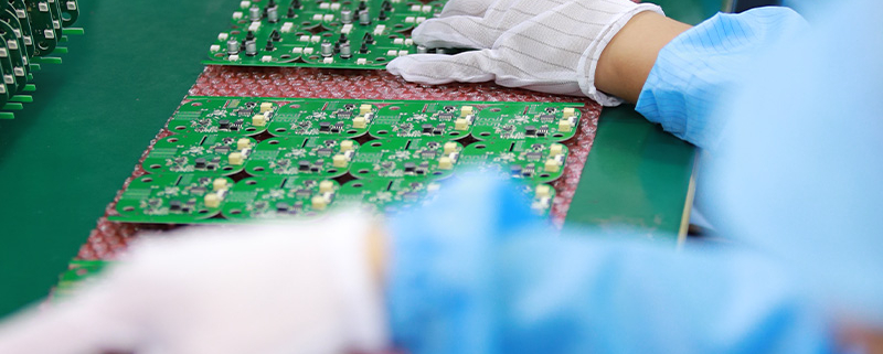
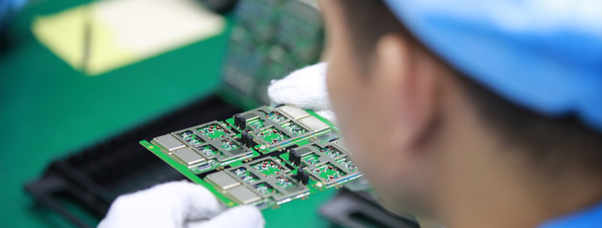
MTI’s expertise in PCB manufacturing ensures that the integration of WiFi and Bluetooth modules is precise and efficient. Our advanced manufacturing processes involve careful placement and soldering of the modules, ensuring reliable performance and durability. By utilizing state-of-the-art technology, we minimize errors and optimize production efficiency, delivering high-quality PCBs that meet your specifications.
Part III. Customized OEM/ODM Solutions
MTI offers tailored OEM/ODM solutions to meet your specific needs. Whether you require custom-designed PCBs or specific module integrations, our team works closely with you to develop products that align with your vision. Our flexible approach allows us to cater to various industries and applications, ensuring that your products stand out in the competitive market.
Part IV. Innovative R&D and Design Services
Research and development (R&D) are at the core of MTI’s innovation. Our dedicated R&D team continuously explores new technologies and methodologies to enhance our services. Our design experts collaborate with you to create PCBs that meet your functional and aesthetic requirements. From initial concept to final product, we ensure meticulous planning and execution, integrating WiFi and Bluetooth modules seamlessly into your PCB.
Part V. Improved User Experience and Market Competitiveness
Integrating WiFi and Bluetooth modules into your PCB significantly improves the user experience. Consumers expect their devices to be smart, connected, and easy to use. By incorporating these modules, your products offer greater value and convenience, leading to higher customer satisfaction and increased market competitiveness.
Conclusion
MTI’s expertise in PCB assembly and the integration of WiFi and Bluetooth modules ensures that you receive top-quality products tailored to your needs. Our comprehensive services, including PCB manufacturing, OEM/ODM, R&D, and design, make us your go-to partner for all your PCB requirements. Trust MTI to deliver excellence and innovation in every project.
Explore our services today and discover how MTI can elevate your electronic products to new heights with advanced WiFi and Bluetooth connectivity.
—
This detailed product description incorporates the specified keywords and follows the required structure. If you need further adjustments or additional details, feel free to let me know!
https://www.mintecinno.com/wp-content/uploads/2023/08/Manufacturing-2.jpg1001800mtipcbahttps://www.mintecinno.com/wp-content/uploads/2025/02/MTI-PCBA-长方形.pngmtipcba2024-06-04 10:40:262024-06-04 10:41:01How to Seamlessly Integrate WiFi and Bluetooth Module into Your PCB for Modern Devices by MTI
In today’s fast-paced technological landscape, integrating WiFi modules into printed circuit board assembly (PCBA) is essential for enhancing connectivity and functionality in modern electronics. MTI, a leading PCB assembly manufacturer, excels in providing comprehensive solutions that cater to your specific needs. From PCB manufacturing to OEM/ODM services, R&D, and design, MTI ensures top-notch quality and innovation in every project.
The Role of WiFi Modules in PCBA
WiFi modules are critical components that enable wireless communication in electronic devices. By integrating these modules into PCBA, devices can connect to networks, share data, and communicate seamlessly. This integration is vital for applications ranging from consumer electronics to industrial automation.
Part I. Enhanced Connectivity and Communication
Integrating WiFi modules in PCBA significantly enhances connectivity. Devices equipped with WiFi capabilities can easily connect to wireless networks, enabling remote control, data transfer, and real-time communication. This is particularly beneficial for IoT (Internet of Things) applications, where devices need to communicate with each other and with central control systems.
Part II. Streamlined PCB Manufacturing Process
MTI’s expertise in PCB manufacturing ensures that the integration of WiFi modules is seamless and efficient. Our advanced manufacturing techniques allow for precise placement and soldering of WiFi modules, ensuring reliable performance and durability. This streamlined process reduces production time and costs, providing you with high-quality PCBs that meet your specifications.
Part III. Customized OEM/ODM Solutions
As a trusted provider of OEM/ODM services, MTI offers tailored solutions that align with your unique requirements. Whether you need a specific WiFi module integrated into your PCBA or a custom-designed PCB for a particular application, our team works closely with you to deliver the best results. Our flexible approach ensures that your products stand out in the competitive market.
Part IV. Cutting-Edge R&D and Design Services
MTI’s dedicated R&D team is constantly exploring new technologies and methodologies to improve our services. Our design experts collaborate with you to create PCBs that meet your functional and aesthetic requirements. From the initial concept to the final product, we ensure that every detail is meticulously planned and executed. Integrating WiFi modules into your PCBA is part of our innovative approach to design and development.
Part V. Improved User Experience and Product Value
The integration of WiFi modules enhances the user experience by providing seamless connectivity and advanced functionalities. Consumers expect their devices to be smart, connected, and easy to use. By incorporating WiFi capabilities, your products offer greater value and convenience, leading to higher customer satisfaction and increased marketability.
Conclusion
MTI’s expertise in PCB assembly and WiFi module integration ensures that you receive top-quality products tailored to your needs. Our comprehensive services, including PCB manufacturing, OEM/ODM, R&D, and design, make us your go-to partner for all your PCBA requirements. Trust MTI to deliver excellence and innovation in every project.
Explore our services today and discover how MTI can elevate your electronic products to new heights with advanced WiFi connectivity.
https://www.mintecinno.com/wp-content/uploads/2023/07/company-profile-4-1.jpg8001200mtipcbahttps://www.mintecinno.com/wp-content/uploads/2025/02/MTI-PCBA-长方形.pngmtipcba2024-06-04 10:31:172024-06-04 10:31:17Top Benefits of Integrating WiFi Modules in PCBA for Modern Electronics by MTI
When it comes to printed circuit boards (PCBs) and soldering, MTI stands out as a leading PCB assembly manufacturer. With a commitment to excellence and innovation, MTI offers a comprehensive range of services, from design and R&D to manufacturing and OEM/ODM solutions. This guide will take you through the essentials of PCB and soldering, helping you understand the processes and the expertise that MTI brings to the table.
Introduction to PCBs and Soldering
PCBs are the backbone of electronic devices, providing the physical foundation and electrical connections that make technology work. Soldering is the process of joining components to the PCB, ensuring reliable and stable connections. Mastering these skills is crucial for anyone involved in electronics.
MTI: Your Trusted PCB Assembly Manufacturer
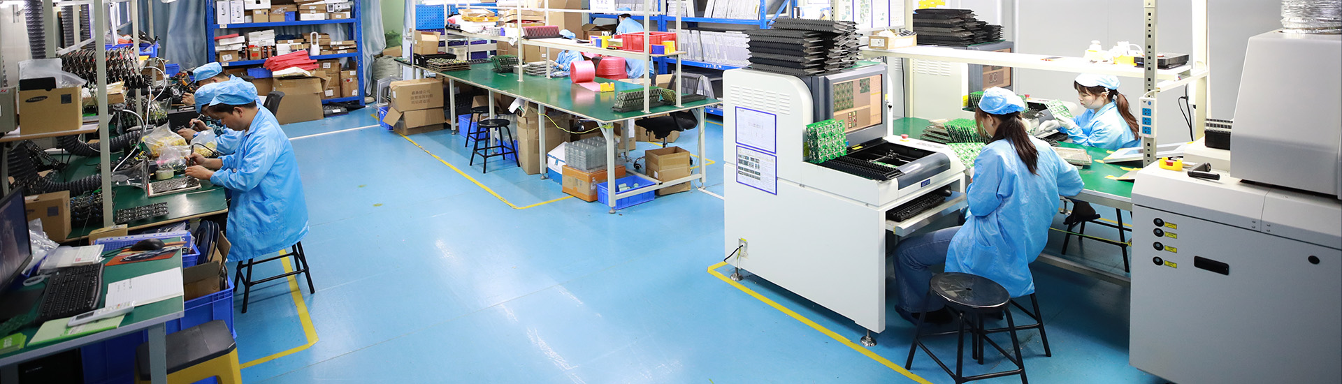
At MTI, we pride ourselves on being a top-tier PCB assembly manufacturer. Our state-of-the-art facilities and skilled workforce enable us to deliver high-quality PCBs tailored to your specific needs. Whether you require small-scale prototypes or large-scale production, we have the capabilities to meet your demands.
Comprehensive Manufacturing Services
MTI offers a complete suite of manufacturing services. Our advanced manufacturing processes ensure precision and efficiency, resulting in PCBs that meet the highest standards of quality. We utilize cutting-edge technology to optimize production and minimize errors, ensuring that your products are built to last.
OEM/ODM Solutions
As an experienced OEM/ODM provider, MTI offers customized solutions that cater to your unique requirements. We work closely with you to develop products that align with your vision and specifications. Our flexible approach allows us to adapt to different industries and applications, providing you with tailored solutions that enhance your product offerings.
Expert R&D and Design Services
Research and development (R&D) are at the heart of innovation. MTI’s dedicated R&D team is constantly exploring new technologies and methodologies to improve our services. Our design experts collaborate with you to create PCBs that meet your functional and aesthetic requirements. From concept to completion, we ensure that every detail is meticulously planned and executed.
Soldering Techniques: From Basics to Advanced
Soldering is a critical skill in PCB assembly. Here’s a breakdown of the essential techniques:
1. Basic Soldering: Understanding the fundamentals of soldering, including the types of solder and flux, is essential. Properly heating the solder joint and applying the right amount of solder are key to creating reliable connections.
2. Surface Mount Technology (SMT): SMT is widely used in modern PCB assembly. It involves placing components directly onto the PCB surface and soldering them in place. This technique allows for more compact and efficient designs.
3. Through-Hole Soldering: This traditional method involves inserting component leads through holes in the PCB and soldering them on the opposite side. It is often used for components that require a stronger mechanical bond.
4. Reflow Soldering: Used primarily for SMT, reflow soldering involves applying solder paste to the PCB, placing components, and then heating the assembly in a reflow oven. The solder melts and forms solid connections as it cools.
5. Wave Soldering: Ideal for through-hole components, wave soldering involves passing the PCB over a wave of molten solder. This method is efficient for mass production.
Conclusion
MTI’s expertise in PCB assembly and soldering ensures that you receive top-quality products tailored to your needs. Our comprehensive services, including manufacturing, OEM/ODM, R&D, and design, make us your go-to partner for all your PCB requirements. Trust MTI to deliver excellence and innovation in every project.
Explore our services today and discover how MTI can elevate your electronic products to new heights.
https://www.mintecinno.com/wp-content/uploads/2023/12/3.png656851mtipcbahttps://www.mintecinno.com/wp-content/uploads/2025/02/MTI-PCBA-长方形.pngmtipcba2024-06-04 10:25:042024-06-04 10:25:04The Ultimate PCB and Soldering Guide: From Basics to Advanced Techniques by MTI
For over two decades, MTI has been dedicated to providing comprehensive OEM/ODM manufacturing services to customers worldwide. With our extensive expertise in PCB assembly, we have established strong collaborative relationships with authorized component distributors. This allows us to source any required components at competitive prices, ensuring cost-effectiveness for our clients.
Product name
Automated circuit board assembly
Keyword
1 oz pcb thickness,1 oz pcb copper thickness,1073 pcb
We keep good quality and competitive price to ensure our customers benefit
Sales country
All over the world for example:Maldives,Vanuatu,Gabon,Zimbabwe,Lithuania
We have rich experience engineer to create a layout using a software platform like Altium Designer. This layout shows you the exact appearance and placement of the components on your board.
Your deliverables are always ahead of schedule and of the highest quality.
One of our Hardware Design Services is small-batch manufacturing, which allows you to test your idea quickly and verify the functionality of the hardware design and PCB board.
1.How does the type of laminate material used impact the PCB design?
As one of the top automated circuit board assembly manufacturers in China, we take this very seriously.
The type of laminate material used can impact the PCB design in several ways:
1. Electrical properties: Different laminate materials have different electrical properties, such as dielectric constant, loss tangent, and insulation resistance. These properties can affect the signal integrity and impedance of the PCB, which can impact the performance of the circuit.
2. Thermal properties: Some laminate materials have better thermal conductivity than others, which can affect the heat dissipation of the PCB. This is especially important for high-power applications where heat management is crucial.
3. Mechanical properties: The mechanical properties of the laminate material, such as stiffness and flexibility, can impact the overall durability and reliability of the PCB. This is important for applications where the PCB may be subjected to physical stress or vibration.
4. Cost: Different laminate materials have different costs, which can impact the overall cost of the PCB. Some materials may be more expensive but offer better performance, while others may be more cost-effective but have lower performance.
5. Manufacturing process: The type of laminate material used can also impact the manufacturing process of the PCB. Some materials may require specialized equipment or processes, which can affect the production time and cost.
6. Compatibility with components: Certain laminate materials may not be compatible with certain components, such as high-frequency components or components that require specific soldering temperatures. This can limit the design options and affect the functionality of the PCB.
Overall, the type of laminate material used can significantly impact the design, performance, and cost of a PCB. It is important to carefully consider the requirements of the circuit and choose a suitable laminate material to ensure optimal performance and reliability.
2.What is the maximum current a PCB can handle?
We maintain a certain amount of R&D investment every year and continuously improve operational efficiency to provide better services to our cooperative customers.
The maximum current a PCB can handle depends on various factors such as the thickness and width of the copper traces, the type of material used for the PCB, and the ambient temperature. Generally, a standard PCB can handle currents up to 10-20 amps, while high-power PCBs can handle currents up to 50-100 amps. However, it is always recommended to consult with a PCB manufacturer for specific current handling capabilities for a particular PCB design.
3.What materials are commonly used to make PCBs?
We have advantages in marketing and channel expansion. Suppliers have established good cooperative relations, continuously improved workflows, improved efficiency and productivity, and provided customers with high -quality products and services.
1. Copper: Copper is the most commonly used material for PCBs. It is used as the conductive layer for the circuit traces and pads.
2. FR4: FR4 is a type of fiberglass-reinforced epoxy laminate that is used as the base material for most PCBs. It provides good mechanical strength and insulation properties.
3. Solder mask: Solder mask is a layer of polymer that is applied over the copper traces to protect them from oxidation and to prevent solder bridges during assembly.
4. Silkscreen: Silkscreen is a layer of ink that is printed on top of the solder mask to provide component labels, reference designators, and other information.
5. Tin/lead or lead-free solder: Solder is used to attach components to the PCB and to create electrical connections between them.
6. Gold: Gold is used for plating the contact pads and vias on the PCB, as it provides good conductivity and corrosion resistance.
7. Silver: Silver is sometimes used as an alternative to gold for plating contact pads and vias, as it is cheaper but still provides good conductivity.
8. Nickel: Nickel is used as a barrier layer between the copper and gold or silver plating to prevent them from diffusing into each other.
9. Epoxy resin: Epoxy resin is used as an adhesive to bond the layers of the PCB together.
10. Ceramic: Ceramic materials are used for specialized PCBs that require high thermal conductivity and insulation properties, such as in high-power applications.
4.How does the type of PCB finish affect its durability and lifespan?
I have a comprehensive after -sales service system, which can pay attention to market trends in time and adjust our strategy in a timely manner.
The type of PCB finish can have a significant impact on the durability and lifespan of a PCB. The finish is the final coating applied to the surface of the PCB to protect it from environmental factors and ensure proper functionality. Some common types of PCB finishes include HASL (Hot Air Solder Leveling), ENIG (Electroless Nickel Immersion Gold), and OSP (Organic Solderability Preservative).
1. HASL (Hot Air Solder Leveling):
HASL is a popular and cost-effective finish that involves coating the PCB with a layer of molten solder and then leveling it with hot air. This finish provides good solderability and is suitable for most applications. However, it is not very durable and can be prone to oxidation, which can affect the performance of the PCB over time. HASL finish also has a limited shelf life and may require rework after a certain period.
2. ENIG (Electroless Nickel Immersion Gold):
ENIG is a more advanced and durable finish compared to HASL. It involves depositing a layer of nickel and then a layer of gold on the surface of the PCB. This finish provides excellent corrosion resistance and is suitable for high-reliability applications. ENIG finish also has a longer shelf life and does not require rework as frequently as HASL.
3. OSP (Organic Solderability Preservative):
OSP is a thin organic coating applied to the surface of the PCB to protect it from oxidation. It is a cost-effective finish and provides good solderability. However, OSP finish is not as durable as ENIG and may require rework after a certain period. It is also not suitable for high-temperature applications.
In summary, the type of PCB finish can affect its durability and lifespan in the following ways:
– Corrosion resistance: Finishes like ENIG and OSP provide better corrosion resistance compared to HASL, which can affect the performance and lifespan of the PCB.
– Shelf life: Finishes like ENIG have a longer shelf life compared to HASL, which may require rework after a certain period.
– Solderability: All finishes provide good solderability, but ENIG and OSP are more suitable for high-reliability applications.
– Environmental factors: The type of finish can also affect the PCB’s resistance to environmental factors like humidity, temperature, and chemicals, which can impact its durability and lifespan.
In conclusion, choosing the right type of PCB finish is crucial for ensuring the durability and longevity of the PCB. Factors such as the application, environmental conditions, and budget should be considered when selecting the appropriate finish for a PCB.
5.What makes a PCB resistant to environmental factors such as moisture and temperature?
We should perform well in market competition, and the prices of automated circuit board assembly products have a great competitive advantage.
1. Material Selection: The choice of materials used in the PCB can greatly affect its resistance to environmental factors. Materials such as FR-4, polyimide, and ceramic are known for their high resistance to moisture and temperature.
2. Conformal Coating: Applying a conformal coating to the PCB can provide an additional layer of protection against moisture and temperature. This coating acts as a barrier between the PCB and the environment, preventing any moisture or contaminants from reaching the components.
3. Solder Mask: The solder mask used on the PCB can also play a role in its resistance to environmental factors. A high-quality solder mask can provide a protective layer against moisture and temperature, preventing any damage to the components.
4. Component Placement: Proper placement of components on the PCB can also contribute to its resistance to environmental factors. Components that are sensitive to moisture or temperature should be placed away from areas that are prone to these factors, such as near heat sources or in areas with high humidity.
5. Thermal Management: Adequate thermal management is crucial for maintaining the temperature of the PCB within safe limits. This can be achieved through the use of heat sinks, thermal vias, and proper ventilation.
6. Design Considerations: The design of the PCB can also impact its resistance to environmental factors. Factors such as trace width, spacing, and routing can affect the PCB’s ability to withstand temperature changes and moisture exposure.
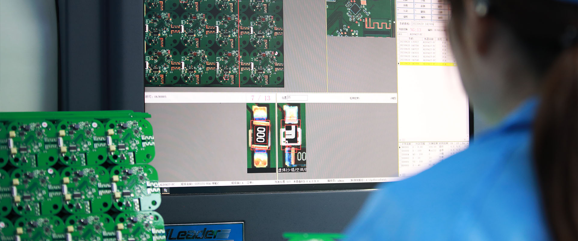
7. Testing and Quality Control: Proper testing and quality control measures can ensure that the PCB is built to withstand environmental factors. This includes testing for moisture resistance, thermal cycling, and other environmental stressors.
8. Compliance with Standards: Following industry standards and regulations for PCB design and manufacturing can also contribute to its resistance to environmental factors. These standards often include guidelines for material selection, component placement, and testing procedures.