MTI is a leading PCB assembly Manufacturer
known for its advanced technology, high-quality products, and exceptional customer service. As a key player in the electronics industry, we understand the nuances of PCB manufacturing and fabrication. This article aims to clarify the difference between these two essential processes, providing insight into how MTI leverages both to deliver superior PCBs to our clients.
Understanding PCB Fabrication
What is PCB Fabrication?
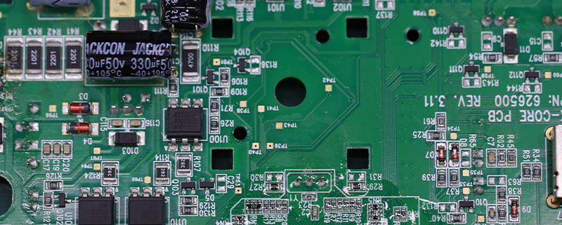
PCB fabrication is the process of creating the physical circuit board that will later be used in electronic devices. This involves several steps, including the design, layout, and etching of the board to form the necessary electrical pathways.
Key Steps in PCB Fabrication
Design and Layout
: The initial phase involves creating a detailed design and layout of the PCB using specialized CAD software. This design includes all the necessary electrical connections and component placements.
Material Selection
: Choosing the right materials is crucial for the board’s performance. Common materials include FR4 (a type of fiberglass), metal, and high-frequency laminates.
Etching and Layering
: The design is transferred onto the board material, and unwanted copper is etched away to create the electrical pathways. Multi-layer boards involve adding and laminating multiple layers of these etched designs.
Drilling
: Precise holes are drilled for component leads and vias (vertical interconnect accesses) to connect different layers of the board.
Plating and Solder Mask Application
: Copper plating is applied to the drilled holes, and a solder mask is added to protect the board and prevent solder bridges.
Advantages of PCB Fabrication
PCB fabrication is a highly specialized process that ensures the foundational integrity of the circuit board. By focusing on quality materials and precision engineering, MTI guarantees that the fabricated boards meet the highest standards of durability and performance.
Cost Performance
Efficient fabrication processes and high-quality materials contribute to excellent cost performance, making MTI’s PCBs a cost-effective choice for wholesalers, distributors, and OEM/ODM clients.
Understanding PCB Manufacturing
What is PCB Manufacturing?
PCB manufacturing encompasses the entire process of bringing a PCB design to life, including both the fabrication of the board itself and the assembly of electronic components onto the board. This comprehensive process ensures that the final product is ready for integration into electronic devices.
Key Steps in PCB Manufacturing
Fabrication
: As described above, this is the creation of the physical board.
Component Sourcing
: Sourcing the necessary electronic components from reliable suppliers. This involves procuring items like resistors, capacitors, integrated circuits, and connectors.
Assembly
: The components are placed and soldered onto the fabricated board. This can be done using Surface Mount Technology (SMT) or Through-Hole Technology (THT), depending on the design requirements.
Inspection and Testing
: Rigorous testing is conducted to ensure that the assembled PCB functions correctly. This includes electrical tests, functional tests, and visual inspections.
Quality Assurance
: Final quality checks are performed to ensure that the PCBs meet all specifications and standards before shipping to customers.
Advantages of PCB Manufacturing
By handling both fabrication and assembly, MTI ensures seamless integration of all processes, leading to higher quality and reliability in the final product. This comprehensive approach allows us to meet the diverse needs of our clients, from small-scale projects to large OEM/ODM orders.
End-to-End Solutions
Providing end-to-end solutions from design to final assembly enhances our ability to control quality and reduce lead times. This integration is a significant advantage for clients seeking reliable and timely delivery of their PCBs.
Key Differences Between PCB Manufacturing and PCB Fabrication
Scope of Work
PCB Fabrication
: Focuses solely on creating the physical board.
PCB Manufacturing
: Encompasses fabrication plus the assembly of electronic components onto the board.
Processes Involved
PCB Fabrication
: Involves design, material selection, etching, drilling, plating, and solder mask application.
PCB Manufacturing
: Includes all fabrication processes plus component sourcing, assembly, inspection, and quality assurance.
End Product
PCB Fabrication
: Results in a bare board with no components.
PCB Manufacturing
: Delivers a fully assembled and tested PCB ready for use in electronic devices.
Conclusion
Understanding the difference between PCB fabrication and PCB manufacturing is crucial for selecting the right services for your project. At MTI, we offer comprehensive PCB manufacturing solutions that ensure high-quality, reliable, and cost-effective products. Our advanced R&D capabilities, efficient manufacturing processes, and commitment to customer satisfaction make us the ideal partner for all your PCB needs. Whether you are a supplier, agent, or OEM/ODM client, MTI has the expertise and resources to meet your requirements and exceed your expectations.
https://www.mintecinno.com/wp-content/uploads/2023/08/supply-chain.jpg10001500mtipcbahttps://www.mintecinno.com/wp-content/uploads/2025/02/MTI-PCBA-长方形.pngmtipcba2024-07-06 06:09:002024-07-06 06:09:00Difference Between PCB Manufacturing and PCB Fabrication
MTI, a leading PCB assembly Manufacturer
, is proud to present our special PCB designed for cutting-edge technologies. Our commitment to innovation, quality, and precision ensures that our PCBs meet the highest industry standards. Whether you are an OEM/ODM client, a wholesaler, or a distributor, MTI’s PCBs offer unparalleled performance and reliability for a wide range of advanced applications.
Features of MTI’s Special PCB
Advanced Design and Engineering
At MTI, our R&D team continuously pushes the boundaries of PCB design and engineering. Our special PCBs are crafted to support the most demanding technological applications, ensuring optimal performance and durability.
High-Density Interconnect (HDI)
Our PCBs utilize High-Density Interconnect technology, which allows for more components to be placed on a smaller board. This feature is crucial for modern electronics that require compact, efficient, and powerful circuit boards.
Superior Manufacturing Techniques
MTI’s state-of-the-art manufacturing facilities in China are equipped with the latest technology to produce high-quality PCBs. Our precision manufacturing processes ensure that each board meets stringent quality standards.
Multi-Layer PCB Production
We specialize in multi-layer PCB production, which is essential for complex electronics that need multiple layers of circuitry. Our advanced manufacturing techniques ensure that these layers are seamlessly integrated for maximum performance and reliability.
Customization and Flexibility
We offer extensive customization options to meet the unique needs of our clients. Our OEM/ODM services allow for tailored solutions that align perfectly with specific project requirements.
Tailored Solutions
Our team works closely with clients to develop customized PCBs that address unique operational challenges. From specific material selections to unique design requirements, we provide solutions that enhance performance and functionality.
Benefits of MTI’s Special PCB
Enhanced Performance and Reliability
Our special PCBs are designed to deliver superior performance and reliability, making them ideal for cutting-edge technologies. The advanced materials and manufacturing techniques we use ensure that our PCBs can handle the most demanding applications.
Robust and Durable
MTI’s PCBs are built to last, with robust materials and construction that ensure durability even in harsh conditions. This reliability is a significant advantage for businesses that require consistent and dependable performance from their electronics.
Cost Performance
By leveraging advanced manufacturing techniques and maintaining efficient operations, we offer competitive pricing on all our PCBs. This cost performance makes MTI an attractive supplier for businesses looking for high-quality, affordable PCBs.
Efficient Production
Our efficient production processes reduce waste and lower costs, allowing us to pass these savings on to our clients. This makes our PCBs a cost-effective solution for a wide range of applications.
Versatile Applications
MTI’s special PCBs are suitable for a variety of advanced technologies, from consumer electronics to industrial applications. Their versatility makes them a valuable component in numerous cutting-edge projects.
Broad Industry Use
Our PCBs are used in various industries, including telecommunications, aerospace, medical devices, and more. Their adaptability and high performance make them suitable for any application requiring advanced circuit board technology.
Reliable Supply Chain
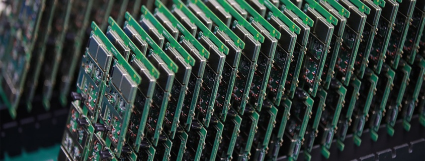
As a trusted manufacturer, MTI ensures a reliable supply chain that can meet the demands of businesses of all sizes. Our production capacity and logistical expertise enable us to handle large orders with ease, ensuring timely delivery and consistent quality.
Dedicated Support and Service
Our dedicated support team is always available to assist with any queries or issues. We pride ourselves on our responsive and knowledgeable service, ensuring that our clients receive the best possible experience.
Why Choose MTI?
Innovation and Quality
At MTI, we prioritize innovation and quality in all our products. Our special PCBs are a testament to our commitment to delivering cutting-edge solutions that meet the evolving needs of the industry.
Rigorous Testing and Quality Control
All our PCBs undergo rigorous testing and quality control processes to ensure they meet the highest standards. This dedication to quality ensures that our clients receive reliable and durable products that perform as expected.
Sustainable Practices
We are committed to sustainable manufacturing practices. Our factory utilizes eco-friendly processes and materials, reducing our environmental impact and promoting sustainability.
Responsible Sourcing
We source materials responsibly and work with suppliers who share our commitment to sustainability. This ensures that our PCBs not only perform well but also align with the values of environmentally conscious clients.
Conclusion
MTI’s special PCBs are designed for cutting-edge technologies, offering superior performance, reliability, and customization options. As a leading PCB assembly manufacturer, we are dedicated to delivering innovative products and exceptional support to our clients. Partner with MTI to experience the advantages of our advanced PCBs and elevate your technological projects to new heights.
For over two decades, MTI has been dedicated to providing comprehensive OEM/ODM manufacturing services to customers worldwide. With our extensive expertise in PCB assembly, we have established strong collaborative relationships with authorized component distributors. This allows us to source any required components at competitive prices, ensuring cost-effectiveness for our clients.
We keep good quality and competitive price to ensure our customers benefit
Sales country
All over the world for example:American Samoa,United Arab Emirates,Yemen,French Guiana,Uganda,Bahrain,Moldova
One of our Hardware Design Services is small-batch manufacturing, which allows you to test your idea quickly and verify the functionality of the hardware design and PCB board.
Your deliverables are always ahead of schedule and of the highest quality.
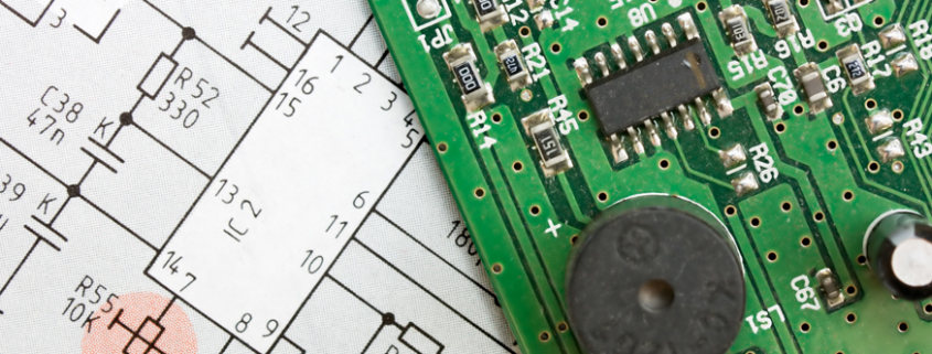
We have rich experience engineer to create a layout using a software platform like Altium Designer. This layout shows you the exact appearance and placement of the components on your board.
1.What are the advantages and disadvantages of using a rigid or flexible PCB?
We have the leading technology and innovation capabilities, and attach importance to employee training and development, and provide promotion opportunities.
Advantages of rigid PCB:
1. Durability: Rigid PCBs are more durable and can withstand higher levels of stress and strain compared to flexible PCBs.
2. Better for high-speed applications: Rigid PCBs are better suited for high-speed applications as they have better signal integrity and lower signal loss.
3. Cost-effective: Rigid PCBs are generally less expensive to manufacture compared to flexible PCBs.
4. Easier to assemble: Rigid PCBs are easier to assemble and can be used with automated assembly processes, making them more efficient for mass production.
5. Higher component density: Rigid PCBs can accommodate a higher number of components and have a higher component density compared to flexible PCBs.
Disadvantages of rigid PCB:
1. Limited flexibility: Rigid PCBs are not flexible and cannot be bent or twisted, making them unsuitable for certain applications.
2. Bulkier: Rigid PCBs are bulkier and take up more space compared to flexible PCBs, which can be a disadvantage in compact electronic devices.
3. Prone to damage: Rigid PCBs are more prone to damage from vibrations and shocks, which can affect their performance.
Advantages of flexible PCB:
1. Flexibility: Flexible PCBs can be bent, twisted, and folded, making them suitable for applications where space is limited or where the PCB needs to conform to a specific shape.
2. Lightweight: Flexible PCBs are lightweight and take up less space compared to rigid PCBs, making them ideal for portable electronic devices.
3. Better for high vibration environments: Flexible PCBs are more resistant to vibrations and shocks, making them suitable for use in high vibration environments.
4. Higher reliability: Flexible PCBs have fewer interconnects and solder joints, reducing the chances of failure and increasing reliability.
Disadvantages of flexible PCB:
1. Higher cost: Flexible PCBs are generally more expensive to manufacture compared to rigid PCBs.
2. Limited component density: Flexible PCBs have a lower component density compared to rigid PCBs, which can limit their use in high-density applications.
3. Difficult to repair: Flexible PCBs are more difficult to repair compared to rigid PCBs, as they require specialized equipment and expertise.
4. Less suitable for high-speed applications: Flexible PCBs have higher signal loss and lower signal integrity compared to rigid PCBs, making them less suitable for high-speed applications.
2.What materials are commonly used to make PCBs?
We have advantages in marketing and channel expansion. Suppliers have established good cooperative relations, continuously improved workflows, improved efficiency and productivity, and provided customers with high -quality products and services.
1. Copper: Copper is the most commonly used material for PCBs. It is used as the conductive layer for the circuit traces and pads.
2. FR4: FR4 is a type of fiberglass-reinforced epoxy laminate that is used as the base material for most PCBs. It provides good mechanical strength and insulation properties.
3. Solder mask: Solder mask is a layer of polymer that is applied over the copper traces to protect them from oxidation and to prevent solder bridges during assembly.
4. Silkscreen: Silkscreen is a layer of ink that is printed on top of the solder mask to provide component labels, reference designators, and other information.
5. Tin/lead or lead-free solder: Solder is used to attach components to the PCB and to create electrical connections between them.
6. Gold: Gold is used for plating the contact pads and vias on the PCB, as it provides good conductivity and corrosion resistance.
7. Silver: Silver is sometimes used as an alternative to gold for plating contact pads and vias, as it is cheaper but still provides good conductivity.
8. Nickel: Nickel is used as a barrier layer between the copper and gold or silver plating to prevent them from diffusing into each other.
9. Epoxy resin: Epoxy resin is used as an adhesive to bond the layers of the PCB together.
10. Ceramic: Ceramic materials are used for specialized PCBs that require high thermal conductivity and insulation properties, such as in high-power applications.
3.How does the type of PCB connection (wired or wireless) impact its design and features?
Our products & services cover a wide range of areas and meet the needs of different fields.
The type of PCB connection, whether wired or wireless, can have a significant impact on the design and features of the PCB. Some of the key ways in which the type of connection can impact the PCB design and features are:
1. Size and form factor: Wired PCBs typically require physical connectors and cables, which can add to the overall size and form factor of the PCB. On the other hand, wireless PCBs do not require physical connectors and cables, allowing for a smaller and more compact design.
2. Power consumption: Wired PCBs require a constant supply of power to function, whereas wireless PCBs can operate on battery power. This can impact the power consumption and battery life of the device, which in turn can affect the overall design and features of the PCB.
3. Flexibility and mobility: Wireless PCBs offer greater flexibility and mobility as they do not have physical connections that restrict movement. This can be advantageous in applications where the device needs to be moved or used in different locations.
4. Data transfer speed: Wired PCBs typically have faster data transfer speeds compared to wireless PCBs. This can impact the design and features of the PCB, as certain applications may require high-speed data transfer.
5. Cost: The type of connection can also impact the cost of the PCB. Wired PCBs may require additional components such as connectors and cables, which can add to the overall cost. Wireless PCBs, on the other hand, may require more advanced technology and components, making them more expensive.
6. Reliability: Wired PCBs are generally considered more reliable as they have a physical connection, which is less prone to interference or signal loss. Wireless PCBs, on the other hand, may be more susceptible to interference and signal loss, which can impact their reliability.
Overall, the type of PCB connection can significantly impact the design and features of the PCB, and it is important to carefully consider the specific requirements of the application when choosing between wired and wireless connections.
4.Can PCBs have different shapes and sizes?
Our company has many years of flex pcba flexible pcb experience and expertise.
Yes, PCBs (printed circuit boards) can have different shapes and sizes depending on the specific design and purpose of the circuit. They can range from small and compact to large and complex, and can be rectangular, circular, or even irregularly shaped. The shape and size of a PCB is determined by the layout of the components and the desired functionality of the circuit.
5.How does the type of solder mask used affect the PCB’s performance?
We have broad development space in domestic and foreign markets. flex pcba flexible pcbs have great advantages in terms of price, quality, and delivery date.
The type of solder mask used can affect the PCB’s performance in several ways:
1. Insulation: Solder mask is used to insulate the copper traces on a PCB, preventing them from coming into contact with each other and causing a short circuit. The type of solder mask used can affect the level of insulation provided, which can impact the overall reliability and functionality of the PCB.
2. Solderability: Solder mask also plays a crucial role in the soldering process. The type of solder mask used can affect the surface tension and wetting properties of the solder, which can impact the quality of the solder joints and the overall reliability of the PCB.
3. Thermal resistance: Solder mask can also act as a thermal barrier, protecting the PCB from excessive heat. The type of solder mask used can affect the thermal resistance of the PCB, which can impact its ability to dissipate heat and its overall thermal performance.
4. Chemical resistance: Solder mask is also exposed to various chemicals during the PCB manufacturing process, such as flux and cleaning agents. The type of solder mask used can affect its resistance to these chemicals, which can impact the overall durability and reliability of the PCB.
5. Electrical properties: The type of solder mask used can also affect the electrical properties of the PCB, such as its dielectric constant and dissipation factor. These properties can impact the performance of high-frequency circuits and signal integrity.
Overall, the type of solder mask used can have a significant impact on the performance, reliability, and durability of a PCB. It is essential to carefully select the appropriate solder mask for a specific application to ensure optimal performance.
6.What is the maximum current a PCB can handle?
We maintain a certain amount of R&D investment every year and continuously improve operational efficiency to provide better services to our cooperative customers.
The maximum current a PCB can handle depends on various factors such as the thickness and width of the copper traces, the type of material used for the PCB, and the ambient temperature. Generally, a standard PCB can handle currents up to 10-20 amps, while high-power PCBs can handle currents up to 50-100 amps. However, it is always recommended to consult with a PCB manufacturer for specific current handling capabilities for a particular PCB design.
7.Can PCBs be designed with high-speed and high-frequency applications in mind?
We attach importance to the innovation ability and team spirit of employees, have advanced R & D facilities and laboratories, and have a good quality management system.
Yes, PCBs can be designed with high-speed and high-frequency applications in mind. This involves careful consideration of the layout, trace routing, and component placement to minimize signal loss and interference. Specialized materials and techniques, such as controlled impedance routing and differential pairs, can also be used to improve signal integrity and reduce noise. Additionally, the use of advanced simulation and analysis tools can help optimize the design for high-speed and high-frequency performance.
8.How important is the trace width and spacing in a PCB design?
Our flex pcba flexible pcb products have competitive and differentiated advantages, and actively promote digital transformation and innovation.
The trace width and spacing in a PCB design are crucial factors that can greatly affect the performance and reliability of the circuit. Here are some reasons why:
1. Current carrying capacity: The trace width determines the amount of current that can flow through the trace without causing excessive heating. If the trace width is too narrow, it can lead to overheating and damage to the circuit.
2. Voltage drop: The trace width also affects the voltage drop across the trace. A narrow trace will have a higher resistance, resulting in a higher voltage drop. This can cause a decrease in the voltage level at the end of the trace, affecting the performance of the circuit.
3. Signal integrity: The spacing between traces is critical for maintaining signal integrity. If the spacing is too narrow, it can lead to crosstalk and interference between signals, resulting in errors and malfunctions in the circuit.
4. Thermal management: The spacing between traces also plays a role in thermal management. Adequate spacing between traces allows for better air circulation, which helps dissipate heat from the circuit. This is especially important for high-power circuits.
5. Manufacturing constraints: The trace width and spacing also need to be considered in the manufacturing process. If the traces are too close together, it can be challenging to etch and inspect the PCB, leading to manufacturing defects.
In summary, the trace width and spacing are critical parameters that need to be carefully considered in PCB design to ensure proper functioning and reliability of the circuit.
MTI is a manufacturer of high-precision printed circuit board (PCB).We specialize in the manufacture of high precision double-sided and multilayer printed circuit boards, We provide high quality products and faster service for high-tech companies.
We have a group of experienced staff and high-quality management team, set up a complete quality assurance system. Products include FR-4 PCB, Metal PCB and RFPCB (ceramic PCB, PTFE PCB), etc. Have rich experience in the production of thick copper PCB, RF PCB, high Tg PCB, HDI PCB,Fast turn printed circuit board assembly.With ISO9001, ISO14001, TS16949, ISO 13485, RoHS certifications.
We keep good quality and competitive price to ensure our customers benefit
Sales country
All over the world for example:Sweden,United Arab Emirates,Bosnia and Herzegovina,Saint Kitts and Nevis,Cyprus,Navassa Island,Mali,Malawi,Zambia
We have rich experience engineer to create a layout using a software platform like Altium Designer. This layout shows you the exact appearance and placement of the components on your board.
Your deliverables are always ahead of schedule and of the highest quality.
One of our Hardware Design Services is small-batch manufacturing, which allows you to test your idea quickly and verify the functionality of the hardware design and PCB board.
1.How does the number of layers in a PCB affect its functionality?
We should have a stable supply chain and logistics capabilities, and provide customers with high -quality, low -priced fast turn printed circuit board assembly products.
The number of layers in a PCB (Printed Circuit Board) can affect its functionality in several ways:
1. Complexity: The number of layers in a PCB determines the complexity of the circuit design that can be implemented. More layers allow for more components and connections to be included in the design, making it more complex and versatile.
2. Size: A PCB with more layers can be smaller in size compared to a PCB with fewer layers, as it allows for a more compact layout of components and connections. This is especially important in devices with limited space, such as smartphones and wearables.
3. Signal Integrity: The number of layers in a PCB can also affect the signal integrity of the circuit. More layers allow for better routing of signals, reducing the chances of interference and crosstalk between different components.
4. Power Distribution: PCBs with more layers can have dedicated power and ground planes, which help in distributing power evenly across the circuit. This improves the overall performance and stability of the circuit.
5. Cost: The number of layers in a PCB can also affect its cost. More layers mean more materials and manufacturing processes, which can increase the overall cost of the PCB.
6. Thermal Management: PCBs with more layers can have better thermal management, as they allow for the placement of thermal vias and heat sinks to dissipate heat more efficiently. This is important for high-power applications that generate a lot of heat.
In summary, the number of layers in a PCB can significantly impact its functionality, complexity, size, signal integrity, power distribution, cost, and thermal management. Designers must carefully consider the number of layers required for a PCB based on the specific requirements of the circuit and the device it will be used in.
2.What are the advantages and disadvantages of using a rigid or flexible PCB?
We have the leading technology and innovation capabilities, and attach importance to employee training and development, and provide promotion opportunities.
Advantages of rigid PCB:
1. Durability: Rigid PCBs are more durable and can withstand higher levels of stress and strain compared to flexible PCBs.
2. Better for high-speed applications: Rigid PCBs are better suited for high-speed applications as they have better signal integrity and lower signal loss.
3. Cost-effective: Rigid PCBs are generally less expensive to manufacture compared to flexible PCBs.
4. Easier to assemble: Rigid PCBs are easier to assemble and can be used with automated assembly processes, making them more efficient for mass production.
5. Higher component density: Rigid PCBs can accommodate a higher number of components and have a higher component density compared to flexible PCBs.
Disadvantages of rigid PCB:
1. Limited flexibility: Rigid PCBs are not flexible and cannot be bent or twisted, making them unsuitable for certain applications.
2. Bulkier: Rigid PCBs are bulkier and take up more space compared to flexible PCBs, which can be a disadvantage in compact electronic devices.
3. Prone to damage: Rigid PCBs are more prone to damage from vibrations and shocks, which can affect their performance.
Advantages of flexible PCB:
1. Flexibility: Flexible PCBs can be bent, twisted, and folded, making them suitable for applications where space is limited or where the PCB needs to conform to a specific shape.
2. Lightweight: Flexible PCBs are lightweight and take up less space compared to rigid PCBs, making them ideal for portable electronic devices.
3. Better for high vibration environments: Flexible PCBs are more resistant to vibrations and shocks, making them suitable for use in high vibration environments.
4. Higher reliability: Flexible PCBs have fewer interconnects and solder joints, reducing the chances of failure and increasing reliability.
Disadvantages of flexible PCB:
1. Higher cost: Flexible PCBs are generally more expensive to manufacture compared to rigid PCBs.
2. Limited component density: Flexible PCBs have a lower component density compared to rigid PCBs, which can limit their use in high-density applications.
3. Difficult to repair: Flexible PCBs are more difficult to repair compared to rigid PCBs, as they require specialized equipment and expertise.
4. Less suitable for high-speed applications: Flexible PCBs have higher signal loss and lower signal integrity compared to rigid PCBs, making them less suitable for high-speed applications.
3.What are the factors to consider when choosing the right PCB material for a specific application?
We are centered on customers and always pay attention to customers’ needs for fast turn printed circuit board assembly products.
1. Electrical properties: The electrical properties of the PCB material, such as dielectric constant, loss tangent, and insulation resistance, should be carefully considered to ensure optimal performance for the specific application.
2. Thermal properties: The thermal conductivity and coefficient of thermal expansion of the PCB material are important factors to consider, especially for applications that require high power or operate in extreme temperatures.
3. Mechanical properties: The mechanical strength, stiffness, and flexibility of the PCB material should be evaluated to ensure it can withstand the physical stresses and strains of the application.
4. Chemical resistance: The PCB material should be resistant to any chemicals or solvents that it may come into contact with during its use.
5. Cost: The cost of the PCB material should be considered, as it can vary significantly depending on the type and quality of the material.
6. Availability: Some PCB materials may be more readily available than others, which can affect production timelines and costs.
7. Manufacturing process: The chosen PCB material should be compatible with the manufacturing process, such as etching, drilling, and plating, to ensure efficient and reliable production.
8. Environmental factors: The application environment, such as humidity, moisture, and exposure to UV light, should be taken into account when selecting a PCB material to ensure it can withstand these conditions.
9. Signal integrity: For high-frequency applications, the PCB material should have low signal loss and good signal integrity to prevent interference and ensure accurate signal transmission.
10. RoHS compliance: If the application requires compliance with environmental regulations, such as the Restriction of Hazardous Substances (RoHS) directive, the PCB material should be chosen accordingly.
4.Can PCBs be made with different thicknesses?
We operate our fast turn printed circuit board assembly business with integrity and honesty.
Yes, PCBs (printed circuit boards) can be made with different thicknesses. The thickness of a PCB is determined by the thickness of the copper layer and the thickness of the substrate material. The copper layer thickness can range from 0.5 oz to 3 oz, while the substrate material thickness can range from 0.2 mm to 3.2 mm. The most common thicknesses for PCBs are 1.6 mm and 0.8 mm, but custom thicknesses can be requested from PCB manufacturers. The thickness of a PCB can affect its mechanical strength, thermal properties, and electrical performance.
5.What is impedance control and why is it important in PCBs?
We enjoy high authority and influence in the industry and continue to innovate products and service models.
Impedance control is the ability to maintain a consistent electrical impedance throughout a printed circuit board (PCB). It is important in PCBs because it ensures that signals can travel through the board without distortion or loss of quality.
Impedance control is particularly important in high-speed digital and analog circuits, where even small variations in impedance can cause signal reflections and distortions. This can lead to errors in data transmission and affect the overall performance of the circuit.
In addition, impedance control is crucial in ensuring signal integrity and reducing electromagnetic interference (EMI). By maintaining a consistent impedance, the PCB can effectively filter out unwanted signals and prevent them from interfering with the desired signals.
Overall, impedance control is essential for achieving reliable and high-quality performance in PCBs, especially in complex and sensitive electronic systems. It requires careful design and manufacturing techniques, such as controlled trace widths and spacing, to achieve the desired impedance levels.
6.How important is the trace width and spacing in a PCB design?
Our fast turn printed circuit board assembly products have competitive and differentiated advantages, and actively promote digital transformation and innovation.
The trace width and spacing in a PCB design are crucial factors that can greatly affect the performance and reliability of the circuit. Here are some reasons why:
1. Current carrying capacity: The trace width determines the amount of current that can flow through the trace without causing excessive heating. If the trace width is too narrow, it can lead to overheating and damage to the circuit.
2. Voltage drop: The trace width also affects the voltage drop across the trace. A narrow trace will have a higher resistance, resulting in a higher voltage drop. This can cause a decrease in the voltage level at the end of the trace, affecting the performance of the circuit.
3. Signal integrity: The spacing between traces is critical for maintaining signal integrity. If the spacing is too narrow, it can lead to crosstalk and interference between signals, resulting in errors and malfunctions in the circuit.
4. Thermal management: The spacing between traces also plays a role in thermal management. Adequate spacing between traces allows for better air circulation, which helps dissipate heat from the circuit. This is especially important for high-power circuits.
5. Manufacturing constraints: The trace width and spacing also need to be considered in the manufacturing process. If the traces are too close together, it can be challenging to etch and inspect the PCB, leading to manufacturing defects.
In summary, the trace width and spacing are critical parameters that need to be carefully considered in PCB design to ensure proper functioning and reliability of the circuit.
7.How does component placement affect signal integrity in a PCB design?
We pay attention to the transformation of intellectual property protection and innovation achievements. Your OEM or ODM order design we have a complete confidentiality system.
Component placement plays a crucial role in determining the signal integrity of a PCB design. The placement of components affects the routing of traces, which in turn affects the impedance, crosstalk, and signal integrity of the PCB.
1. Impedance: The placement of components affects the impedance of the traces. If components are placed too far apart, the traces will be longer, resulting in higher impedance. This can lead to signal reflections and degradation of the signal.
2. Crosstalk: Crosstalk is the interference between two traces on a PCB. The placement of components can affect the distance between traces, which can increase or decrease crosstalk. If components are placed too close together, the crosstalk between traces can increase, leading to signal distortion.
3. Signal routing: The placement of components also affects the routing of traces. If components are placed in a way that requires traces to make sharp turns or cross over each other, it can result in signal degradation. This can be avoided by carefully placing components in a way that allows for smooth and direct routing of traces.
4. Grounding: Proper grounding is essential for maintaining signal integrity. The placement of components can affect the grounding scheme of the PCB. If components are placed too far from the ground plane, it can result in a longer return path for signals, leading to ground bounce and noise.
5. Thermal considerations: The placement of components can also affect the thermal performance of the PCB. If components that generate a lot of heat are placed too close together, it can result in hot spots and affect the performance of the PCB.
To ensure good signal integrity, it is important to carefully consider the placement of components during the PCB design process. Components should be placed in a way that minimizes trace length, reduces crosstalk, allows for direct routing of traces, and ensures proper grounding and thermal management.
MTI is a professional manufacturer of PCB and PCBA , we supply one-stop service. The company’s main services include PCB production, PCB Assembly and electronic materials purchasing, SMT patch, circuit board welding, circuit board plug-in,eft pcb.
Our clientele spans across major continents (Asia,Europe,Africa,America,Oceania)and encompasses various industries, including healthcare,computer applications
We keep good quality and competitive price to ensure our customers benefit
Sales country
All over the world for example:Turkey,Tunisia,Kuwait,Albania,Burundi,Bangladesh,Australia
One of our Hardware Design Services is small-batch manufacturing, which allows you to test your idea quickly and verify the functionality of the hardware design and PCB board.
We have rich experience engineer to create a layout using a software platform like Altium Designer. This layout shows you the exact appearance and placement of the components on your board.
Your deliverables are always ahead of schedule and of the highest quality.
1.What are the factors to consider when choosing the right PCB material for a specific application?
We are centered on customers and always pay attention to customers’ needs for eft pcb products.
1. Electrical properties: The electrical properties of the PCB material, such as dielectric constant, loss tangent, and insulation resistance, should be carefully considered to ensure optimal performance for the specific application.
2. Thermal properties: The thermal conductivity and coefficient of thermal expansion of the PCB material are important factors to consider, especially for applications that require high power or operate in extreme temperatures.
3. Mechanical properties: The mechanical strength, stiffness, and flexibility of the PCB material should be evaluated to ensure it can withstand the physical stresses and strains of the application.
4. Chemical resistance: The PCB material should be resistant to any chemicals or solvents that it may come into contact with during its use.
5. Cost: The cost of the PCB material should be considered, as it can vary significantly depending on the type and quality of the material.
6. Availability: Some PCB materials may be more readily available than others, which can affect production timelines and costs.
7. Manufacturing process: The chosen PCB material should be compatible with the manufacturing process, such as etching, drilling, and plating, to ensure efficient and reliable production.
8. Environmental factors: The application environment, such as humidity, moisture, and exposure to UV light, should be taken into account when selecting a PCB material to ensure it can withstand these conditions.
9. Signal integrity: For high-frequency applications, the PCB material should have low signal loss and good signal integrity to prevent interference and ensure accurate signal transmission.
10. RoHS compliance: If the application requires compliance with environmental regulations, such as the Restriction of Hazardous Substances (RoHS) directive, the PCB material should be chosen accordingly.
2.What is testability in PCB design and how is it achieved?
Our eft pcb products undergo strict quality control to ensure customer satisfaction.
Testability in PCB design refers to the ease and accuracy with which a printed circuit board (PCB) can be tested for functionality and performance. It is an important aspect of PCB design as it ensures that any defects or issues with the board can be identified and addressed before it is put into use.
Achieving testability in PCB design involves implementing certain design features and techniques that make it easier to test the board. These include:
1. Design for Test (DFT): This involves designing the PCB with specific test points and access points that allow for easy and accurate testing of different components and circuits.
2. Test Points: These are designated points on the PCB where test probes can be connected to measure voltage, current, and other parameters. Test points should be strategically placed to provide access to critical components and circuits.
3. Test Pads: These are small copper pads on the PCB that are used for attaching test probes. They should be placed close to the corresponding component or circuit for accurate testing.
4. Test Jigs: These are specialized tools used for testing PCBs. They can be custom-made for a specific PCB design and can greatly improve the accuracy and efficiency of testing.
5. Design for Manufacturability (DFM): This involves designing the PCB with manufacturing and testing in mind. This includes using standard components, avoiding complex layouts, and minimizing the number of layers to make testing easier.
6. Design for Debug (DFD): This involves designing the PCB with features that make it easier to identify and troubleshoot any issues that may arise during testing.
Overall, achieving testability in PCB design requires careful planning and consideration of the testing process. By implementing DFT, using test points and pads, and designing for manufacturability and debug, designers can ensure that their PCBs are easily testable and can be quickly and accurately diagnosed for any potential issues.
3.How do PCBs support the integration of different electronic components?
We actively participate in the eft pcb industry associations and organization activities. The corporate social responsibility performed well, and the focus of brand building and promotion.
PCBs (Printed Circuit Boards) are essential for the integration of different electronic components in electronic devices. They provide a platform for connecting and supporting the various components, allowing them to work together seamlessly. Here are some ways in which PCBs support the integration of different electronic components:
1. Electrical connections: PCBs have a network of copper traces that connect the different electronic components on the board. These traces act as conductors, allowing electricity to flow between the components and enabling them to communicate and work together.
2. Mounting surface: PCBs provide a stable and secure mounting surface for electronic components. The components are soldered onto the board, ensuring that they are firmly attached and will not move or become loose during operation.
3. Space-saving: PCBs are designed to be compact and space-saving, allowing for the integration of multiple components on a single board. This is especially useful in small electronic devices where space is limited.
4. Customization: PCBs can be customized to accommodate different types and sizes of electronic components. This allows for flexibility in design and the integration of a wide range of components, making it easier to create complex electronic devices.
5. Signal routing: PCBs have multiple layers, with each layer dedicated to a specific function. This allows for efficient routing of signals between components, reducing interference and ensuring that the components can communicate effectively.
6. Power distribution: PCBs have dedicated power planes that distribute power to the different components on the board. This ensures that each component receives the required amount of power, preventing damage and ensuring proper functioning.
7. Thermal management: PCBs also play a crucial role in managing the heat generated by electronic components. They have copper layers that act as heat sinks, dissipating heat and preventing the components from overheating.
In summary, PCBs provide a robust and efficient platform for integrating different electronic components. They enable the components to work together seamlessly, ensuring the proper functioning of electronic devices.
4.How does the number of layers in a PCB affect its functionality?
We should have a stable supply chain and logistics capabilities, and provide customers with high -quality, low -priced eft pcb products.
The number of layers in a PCB (Printed Circuit Board) can affect its functionality in several ways:
1. Complexity: The number of layers in a PCB determines the complexity of the circuit design that can be implemented. More layers allow for more components and connections to be included in the design, making it more complex and versatile.
2. Size: A PCB with more layers can be smaller in size compared to a PCB with fewer layers, as it allows for a more compact layout of components and connections. This is especially important in devices with limited space, such as smartphones and wearables.
3. Signal Integrity: The number of layers in a PCB can also affect the signal integrity of the circuit. More layers allow for better routing of signals, reducing the chances of interference and crosstalk between different components.
4. Power Distribution: PCBs with more layers can have dedicated power and ground planes, which help in distributing power evenly across the circuit. This improves the overall performance and stability of the circuit.
5. Cost: The number of layers in a PCB can also affect its cost. More layers mean more materials and manufacturing processes, which can increase the overall cost of the PCB.
6. Thermal Management: PCBs with more layers can have better thermal management, as they allow for the placement of thermal vias and heat sinks to dissipate heat more efficiently. This is important for high-power applications that generate a lot of heat.
In summary, the number of layers in a PCB can significantly impact its functionality, complexity, size, signal integrity, power distribution, cost, and thermal management. Designers must carefully consider the number of layers required for a PCB based on the specific requirements of the circuit and the device it will be used in.
5.How does the type of PCB connection (wired or wireless) impact its design and features?
Our products & services cover a wide range of areas and meet the needs of different fields.
The type of PCB connection, whether wired or wireless, can have a significant impact on the design and features of the PCB. Some of the key ways in which the type of connection can impact the PCB design and features are:
1. Size and form factor: Wired PCBs typically require physical connectors and cables, which can add to the overall size and form factor of the PCB. On the other hand, wireless PCBs do not require physical connectors and cables, allowing for a smaller and more compact design.
2. Power consumption: Wired PCBs require a constant supply of power to function, whereas wireless PCBs can operate on battery power. This can impact the power consumption and battery life of the device, which in turn can affect the overall design and features of the PCB.
3. Flexibility and mobility: Wireless PCBs offer greater flexibility and mobility as they do not have physical connections that restrict movement. This can be advantageous in applications where the device needs to be moved or used in different locations.
4. Data transfer speed: Wired PCBs typically have faster data transfer speeds compared to wireless PCBs. This can impact the design and features of the PCB, as certain applications may require high-speed data transfer.
5. Cost: The type of connection can also impact the cost of the PCB. Wired PCBs may require additional components such as connectors and cables, which can add to the overall cost. Wireless PCBs, on the other hand, may require more advanced technology and components, making them more expensive.
6. Reliability: Wired PCBs are generally considered more reliable as they have a physical connection, which is less prone to interference or signal loss. Wireless PCBs, on the other hand, may be more susceptible to interference and signal loss, which can impact their reliability.
Overall, the type of PCB connection can significantly impact the design and features of the PCB, and it is important to carefully consider the specific requirements of the application when choosing between wired and wireless connections.


 impact its design and features?")