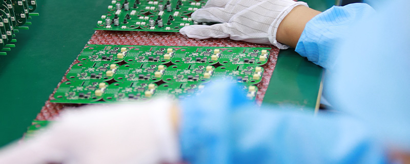
For over two decades, MTI has been dedicated to providing comprehensive OEM/ODM manufacturing services to customers worldwide. With our extensive expertise in PCB assembly, we have established strong collaborative relationships with authorized component distributors. This allows us to source any required components at competitive prices, ensuring cost-effectiveness for our clients.
| Product name | 1 oz pcb thickness |
| Keyword | 1000w amplifier pcb,12v led pcb |
| Place of Origin | China |
| Board Thickness | 2~3.2mm |
| Applicable Industries | industrial control, etc. |
| Service | OEM/ODM manufacturing |
| Certificate | ISO-9001:2015, ISO-14001:2015,ISO-13485:2012.UL/CSA |
| Solder Mask Color | Blue |
| Advantage | We keep good quality and competitive price to ensure our customers benefit |
| Sales country | All over the world for example:Kuwait,Comoros,Ghana,Guernsey,Nepal |
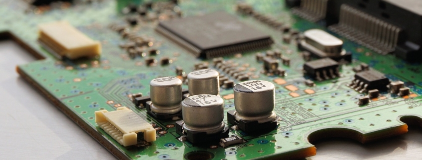
We have rich experience engineer to create a layout using a software platform like Altium Designer. This layout shows you the exact appearance and placement of the components on your board.

Your deliverables are always ahead of schedule and of the highest quality.

One of our Hardware Design Services is small-batch manufacturing, which allows you to test your idea quickly and verify the functionality of the hardware design and PCB board.

FAQs Guide
2.Can a PCB have different levels of flexibility?
3.What are the advantages and disadvantages of using a rigid or flexible PCB?
4.How does the type of signal layers (analog, digital, power) impact the PCB design?
5.What is thermal management in PCBs and why is it important?
1.Can PCBs be customized based on specific design requirements?
We have rich industry experience and professional knowledge, and have strong competitiveness in the market.
Yes, PCBs (printed circuit boards) can be customized based on specific design requirements. This is typically done through the use of computer-aided design (CAD) software, which allows for the creation of a custom layout and design for the PCB. The design can be tailored to meet specific size, shape, and functionality requirements, as well as incorporate specific components and features. The customization process may also involve selecting the appropriate materials and manufacturing techniques to ensure the PCB meets the desired specifications.
2.Can a PCB have different levels of flexibility?
We have a wide range of 1 oz pcb thickness customer groups and establishes long -term cooperative relationships with partners.
Yes, a PCB (printed circuit board) can have different levels of flexibility depending on its design and materials used. Some 1 oz pcb thickness are rigid and cannot bend or flex at all, while others are designed to be flexible and can bend or twist to a certain degree. There are also PCBs that have a combination of rigid and flexible areas, known as flex-rigid PCBs. The level of flexibility in a PCB is determined by factors such as the type of substrate material, the thickness and number of layers, and the type of circuit design.
3.What are the advantages and disadvantages of using a rigid or flexible PCB?
We have the leading technology and innovation capabilities, and attach importance to employee training and development, and provide promotion opportunities.
Advantages of rigid PCB:
1. Durability: Rigid PCBs are more durable and can withstand higher levels of stress and strain compared to flexible PCBs.
2. Better for high-speed applications: Rigid PCBs are better suited for high-speed applications as they have better signal integrity and lower signal loss.
3. Cost-effective: Rigid PCBs are generally less expensive to manufacture compared to flexible PCBs.
4. Easier to assemble: Rigid PCBs are easier to assemble and can be used with automated assembly processes, making them more efficient for mass production.
5. Higher component density: Rigid PCBs can accommodate a higher number of components and have a higher component density compared to flexible PCBs.
Disadvantages of rigid PCB:
1. Limited flexibility: Rigid PCBs are not flexible and cannot be bent or twisted, making them unsuitable for certain applications.
2. Bulkier: Rigid PCBs are bulkier and take up more space compared to flexible PCBs, which can be a disadvantage in compact electronic devices.
3. Prone to damage: Rigid PCBs are more prone to damage from vibrations and shocks, which can affect their performance.
Advantages of flexible PCB:
1. Flexibility: Flexible PCBs can be bent, twisted, and folded, making them suitable for applications where space is limited or where the PCB needs to conform to a specific shape.
2. Lightweight: Flexible PCBs are lightweight and take up less space compared to rigid PCBs, making them ideal for portable electronic devices.
3. Better for high vibration environments: Flexible PCBs are more resistant to vibrations and shocks, making them suitable for use in high vibration environments.
4. Higher reliability: Flexible PCBs have fewer interconnects and solder joints, reducing the chances of failure and increasing reliability.
Disadvantages of flexible PCB:
1. Higher cost: Flexible PCBs are generally more expensive to manufacture compared to rigid PCBs.
2. Limited component density: Flexible PCBs have a lower component density compared to rigid PCBs, which can limit their use in high-density applications.
3. Difficult to repair: Flexible PCBs are more difficult to repair compared to rigid PCBs, as they require specialized equipment and expertise.
4. Less suitable for high-speed applications: Flexible PCBs have higher signal loss and lower signal integrity compared to rigid PCBs, making them less suitable for high-speed applications.
4.How does the type of signal layers (analog, digital, power) impact the PCB design?
As one of the 1 oz pcb thickness market leaders, we are known for innovation and reliability.
The type of signal layers on a PCB (analog, digital, power) can impact the design in several ways:
1. Routing: The type of signal layers will determine how the traces are routed on the 1 oz pcb thickness. Analog signals require careful routing to minimize noise and interference, while digital signals can tolerate more noise. Power signals require wider traces to handle higher currents.
2. Grounding: Analog signals require a solid ground plane to minimize noise and interference, while digital signals can use a split ground plane to isolate sensitive components. Power signals may require multiple ground planes to handle high currents.
3. Component placement: The type of signal layers can also affect the placement of components on the PCB. Analog components should be placed away from digital components to avoid interference, while power components should be placed close to the power source to minimize voltage drops.
4. Signal integrity: The type of signal layers can also impact the signal integrity of the PCB. Analog signals are more susceptible to noise and interference, so the design must take this into account to ensure accurate signal transmission. Digital signals are less sensitive to noise, but the design must still consider signal integrity to avoid timing issues.
5. EMI/EMC: The type of signal layers can also affect the electromagnetic interference (EMI) and electromagnetic compatibility (EMC) of the PCB. Analog signals are more likely to cause EMI/EMC issues, so the design must include measures to reduce these effects. Digital signals are less likely to cause EMI/EMC issues, but the design must still consider these factors to ensure compliance with regulations.
Overall, the type of signal layers on a PCB can significantly impact the design and must be carefully considered to ensure optimal performance and functionality of the circuit.
 impact the PCB design?")
5.What is thermal management in PCBs and why is it important?
We have been working hard to improve service quality and meet customer needs.
Thermal management in PCBs (Printed Circuit Boards) refers to the techniques and strategies used to control and dissipate heat generated by electronic components on the board. It is important because excessive heat can damage components, reduce their performance, and even cause the PCB to fail. Proper thermal management is crucial for ensuring the reliability and longevity of electronic devices.
The electronic components on a PCB generate heat due to the flow of electricity through them. This heat can build up and cause the temperature of the PCB to rise, potentially leading to malfunctions or failures. Thermal management techniques are used to dissipate this heat and maintain the temperature of the PCB within safe operating limits.
There are several methods of thermal management in PCBs, including heat sinks, thermal vias, and thermal pads. Heat sinks are metal components attached to hot components on the PCB to absorb and dissipate heat. Thermal vias are small holes drilled into the PCB to allow heat to escape to the other side of the board. Thermal pads are used to transfer heat from components to the PCB and then to the surrounding air.
Proper thermal management is especially important in high-power and high-density PCBs, where heat generation is more significant. It is also crucial in applications where the PCB is exposed to extreme temperatures or harsh environments. Without effective thermal management, the performance and reliability of electronic devices can be compromised, leading to costly repairs or replacements.
Tags:1.27 mm pcb,104 keyboard pcb,1 oz pcb,2.4 g pcb antenna