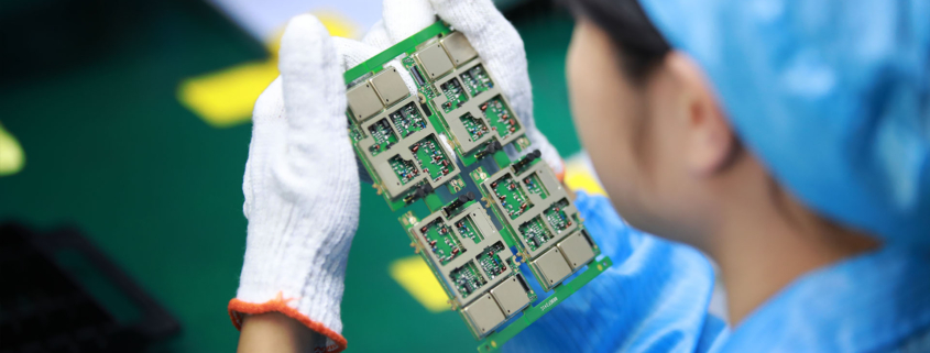
MTI, a leading PCB assembly manufacturer based in China, is dedicated to delivering high-quality PCB assemblies that enhance the overall quality of electronic products. With extensive experience in R&D, design, and manufacturing, MTI offers innovative and cost-effective solutions tailored to meet the diverse needs of our customers. This article explores how PCB assembly manufacturers like MTI improve product quality and highlights the advantages of choosing MTI for your PCB assembly needs.
Ensuring Reliable Performance
Quality in PCB assembly is critical to ensuring the reliable performance of electronic devices. High-quality PCB assemblies contribute to the functionality, durability, and efficiency of the final product, making them essential for manufacturers aiming to deliver superior products.
Meeting Industry Standards
Maintaining high standards in PCB assembly is necessary to comply with industry regulations and standards. This compliance ensures that products are safe, reliable, and perform as expected in various applications.
Advanced R&D and Design Capabilities
Innovative Solutions
PCB assembly manufacturer like MTI invest heavily in R&D to develop innovative solutions that enhance product quality. Our skilled engineers and designers continually explore new materials, technologies, and techniques to improve the performance and reliability of PCB assemblies.
Custom OEM/ODM Services
MTI offers comprehensive OEM/ODM services, allowing customers to create custom PCB assemblies tailored to their specific requirements. This customization ensures that the final product meets the highest standards of quality and performance.
State-of-the-Art Manufacturing Facilities
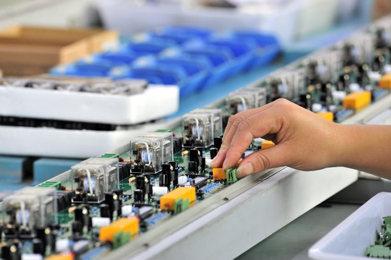
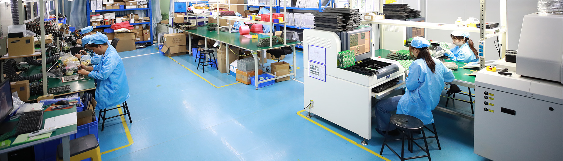
Precision Manufacturing
MTI’s state-of-the-art factory in China is equipped with the latest machinery and technology, enabling us to produce PCB assemblies with high precision and consistency. Our advanced manufacturing processes minimize defects and ensure that every product meets stringent quality standards.
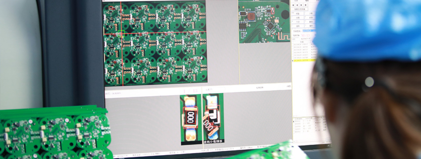
Stringent Quality Control
Our stringent quality control measures include thorough inspections and testing at various stages of the manufacturing process. These measures ensure that each PCB assembly is free from defects and performs reliably in its intended application.
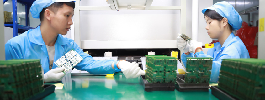
Skilled Workforce
Expertise and Training
MTI’s skilled workforce is trained in the latest manufacturing techniques and quality control procedures. Their expertise and attention to detail ensure that every PCB assembly meets our high standards of quality and reliability.
Continuous Improvement
We believe in continuous improvement and regularly train our staff to stay updated with the latest industry developments and best practices. This commitment to excellence helps us maintain and enhance the quality of our products.
Superior Cost Performance
Competitive Pricing
MTI offers high-quality PCB assemblies at competitive prices. Our efficient manufacturing processes and strategic sourcing enable us to provide cost-effective solutions without compromising on quality.
Long-Term Value
By choosing MTI, you benefit from durable and reliable PCB assemblies that offer long-term value. Our commitment to quality ensures that our products perform efficiently and have a longer lifespan, reducing the total cost of ownership.
Extensive Support and Service
Technical Consultation
MTI provides technical consultation to help customers optimize their PCB designs and assembly processes. Our experts offer valuable insights and recommendations to enhance the performance and efficiency of your electronic products.
Comprehensive Customer Support
Our commitment to customer satisfaction extends beyond the initial sale. MTI offers ongoing support and maintenance services to ensure that our customers continue to receive the best value from their PCB assemblies.
PCB assembly manufacturers like MTI play a crucial role in improving product quality by leveraging advanced R&D, state-of-the-art manufacturing facilities, and stringent quality control measures. MTI’s expertise in design, manufacturing, and continuous improvement ensures that we deliver high-quality PCB assemblies that enhance the performance and reliability of electronic products. Our superior cost performance, comprehensive support, and commitment to excellence make us the ideal partner for your PCB assembly needs.
For more information on our products and services, please contact MTI, your trusted PCB assembly manufacturer.
MTI, a leading PCB assembly manufacturer based in China, is renowned for providing high-quality PCB assembly services to a diverse range of industries. With extensive experience in R&D, design, and manufacturing, MTI offers innovative and cost-effective solutions tailored to meet the specific needs of our customers. This report provides industry insights into PCB assembly manufacturers, highlighting trends, challenges, and the advantages of choosing MTI for your PCB assembly needs.
Growth of Advanced Technologies
Integration of IoT and AI
The PCB assembly industry is witnessing significant growth with the integration of advanced technologies such as the Internet of Things (IoT) and Artificial Intelligence (AI). These technologies are driving demand for more complex and sophisticated PCB designs, pushing manufacturers to innovate continually.
Miniaturization and High-Density Interconnects
There is a growing trend towards miniaturization and high-density interconnect (HDI) technology in PCB assemblies. This trend is fueled by the demand for smaller, more powerful electronic devices, requiring manufacturers to adopt advanced manufacturing techniques and materials.
Focus on Quality and Reliability
Stringent Quality Control
With the increasing complexity of electronic devices, the focus on quality and reliability in PCB assemblies has never been higher. Manufacturers are investing in stringent quality control measures to ensure that their products meet the highest standards of performance and durability.
Environmental Compliance
Sustainability and environmental compliance are becoming critical factors in the PCB assembly industry. Manufacturers are adopting eco-friendly practices and materials to meet regulatory requirements and reduce their environmental footprint.
Supply Chain Disruptions
Component Shortages
The global electronics industry has been facing significant supply chain disruptions, particularly in the availability of semiconductor components. This has posed a challenge for PCB assembly manufacturers in meeting production deadlines and maintaining cost performance.
Logistics and Transportation Issues
Logistics and transportation challenges, exacerbated by the global pandemic, have impacted the timely delivery of components and finished products. Manufacturers need to adopt flexible and resilient supply chain strategies to mitigate these issues.
Increasing Production Costs
Rising Material and Labor Costs
The rising costs of raw materials and labor are putting pressure on PCB assembly manufacturers to maintain competitive pricing while ensuring high-quality output. Efficient manufacturing processes and strategic sourcing are essential to manage these costs effectively.
Technological Advancements
Keeping up with rapid technological advancements requires significant investment in R&D and equipment upgrades. Manufacturers must balance the need for innovation with the financial implications of adopting new technologies.
Expertise and Innovation
Advanced R&D Capabilities
MTI’s advanced R&D capabilities ensure that we stay at the forefront of PCB assembly technology. Our team of skilled engineers and designers continually innovate to deliver high-quality PCB solutions that meet the evolving needs of our customers.
Comprehensive OEM/ODM Services
We offer comprehensive OEM/ODM services, allowing customers to benefit from our expertise and create custom PCB assemblies tailored to their specific requirements. This flexibility ensures that we can meet the unique demands of various industries.
High-Quality Manufacturing Standards
State-of-the-Art Factory
MTI’s state-of-the-art factory in China is equipped with the latest machinery and technology, enabling us to produce high-quality PCB assemblies with precision and efficiency. Our stringent quality control measures ensure that every product meets international standards.
Skilled Workforce
Our skilled workforce is trained in the latest manufacturing techniques and quality control procedures, ensuring that every PCB assembly produced by MTI meets our stringent quality standards.
Superior Cost Performance
Competitive Pricing
MTI offers high-quality PCB assemblies at competitive prices. Our efficient manufacturing processes and strategic sourcing enable us to provide cost-effective solutions without compromising on quality.
Long-Term Value
By choosing MTI, you benefit from durable and reliable PCB assemblies that offer long-term value. Our commitment to quality and innovation ensures that our products perform efficiently and last longer, reducing the total cost of ownership.
Extensive Support and Service
Technical Consultation
MTI provides technical consultation to help customers optimize their PCB designs and assembly processes. Our experts offer valuable insights and recommendations to enhance the performance and efficiency of your electronic products.
Comprehensive Customer Support
Our commitment to customer satisfaction extends beyond the initial sale. MTI offers ongoing support and maintenance services to ensure that our customers continue to receive the best value from their PCB assemblies.
The PCB assembly industry is evolving rapidly, driven by advancements in technology and increasing demands for quality and reliability. MTI’s expertise in R&D, design, and manufacturing positions us as a leader in providing high-quality PCB assembly solutions. Our superior cost performance, comprehensive support, and state-of-the-art facilities make us the ideal partner for your PCB assembly needs.
For more information on our products and services, please contact MTI, your trusted PCB assembly manufacturer.
https://www.mintecinno.com/wp-content/uploads/2023/08/Reliability.jpg8001200mtipcbahttps://www.mintecinno.com/wp-content/uploads/2025/02/MTI-PCBA-长方形.pngmtipcba2024-06-29 08:45:512024-06-29 08:45:51Report on PCB Assembly Manufacturers: Industry Insights
MTI, a leading PCB assembly manufacturer based in China, offers comprehensive PCB copy and PCB design services. With our extensive experience in R&D, design, and manufacturing, we provide innovative and cost-effective solutions tailored to meet the diverse needs of our customers. This article explores the differences between PCB copy and PCB design services and highlights the advantages of choosing MTI for your PCB needs.
What is PCB Copy?
Definition and Process
PCB copy, also known as PCB cloning or reverse engineering, involves duplicating an existing printed circuit board. This process includes analyzing the original PCB, creating a detailed schematic, and producing an exact replica. PCB copy is often used when the original design files are unavailable, or when there is a need to replicate an outdated or discontinued product.
Applications
PCB copy services are commonly used by manufacturers and suppliers who need to reproduce existing products quickly and cost-effectively. This service is particularly beneficial for replacing legacy components or producing spare parts.
What is PCB Design?
Definition and Process
PCB design, on the other hand, involves creating a new printed circuit board from scratch. This process includes conceptualizing the design, creating schematics, laying out the PCB, and prototyping. PCB design is essential for developing new products or improving existing ones.
Applications
PCB design services are ideal for companies involved in R&D and product development. This service allows for the creation of custom PCBs that meet specific requirements and incorporate the latest technologies.
Cost and Time Efficiency
PCB Copy
PCB copy services are generally more cost-effective and faster than PCB design services. Since the design already exists, the process involves minimal R&D, reducing both time and costs. This is an advantage for manufacturers and wholesalers needing quick turnaround times.
PCB Design
PCB design services, while more time-consuming and costly, offer greater flexibility and customization. The design process allows for the incorporation of unique features and optimizations, resulting in a product that perfectly meets the client’s needs.
Flexibility and Customization
PCB Copy
PCB copy services provide limited flexibility as they replicate an existing design. Any modifications or improvements are constrained by the original design’s limitations.
PCB Design
PCB design services offer maximum flexibility and customization. Clients can specify their exact requirements, and the design can be tailored to incorporate new technologies, enhance performance, and improve cost performance.
Intellectual Property Considerations
PCB Copy
PCB copy services must consider intellectual property (IP) issues. Replicating a PCB without proper authorization can lead to legal complications. It is essential to ensure that the original design is not protected by patents or other IP rights.
PCB Design
PCB design services create new, original designs, which can be protected by patents and other IP rights. This protects the client’s investment and provides a competitive advantage in the market.
Expertise and Experience
Advanced R&D Capabilities
MTI’s advanced R&D capabilities ensure that we stay at the forefront of PCB technology. Our team of skilled engineers and designers continuously innovates to deliver high-quality PCB solutions.
Comprehensive OEM/ODM Services
We offer comprehensive OEM/ODM services to meet the specific needs of our clients. Whether you need PCB copy or PCB design services, MTI provides tailored solutions that align with your business goals.
High-Quality Manufacturing Standards
State-of-the-Art Factory
Our state-of-the-art factory in China is equipped with advanced machinery and technology, enabling us to produce high-quality PCBs with precision and efficiency. Our stringent quality control measures ensure that every PCB meets international standards.
Superior Cost Performance
Competitive Pricing
MTI offers competitive pricing without compromising on quality. Our efficient manufacturing processes and strategic sourcing enable us to provide cost-effective PCB solutions.
Long-Term Value
By choosing MTI, you benefit from durable and reliable PCBs that offer long-term value. Our commitment to quality and innovation ensures that our products perform efficiently and last longer, reducing the total cost of ownership.
PCB copy and PCB design services each offer unique advantages, depending on your specific needs. MTI’s expertise in R&D, design, and manufacturing ensures that we can provide high-quality PCB solutions, whether you require an exact replica of an existing board or a custom-designed PCB. Our superior cost performance, comprehensive support, and state-of-the-art facilities make us the ideal partner for your PCB needs.
For more information on our products and services, please contact MTI, your trusted PCB assembly manufacturer.
MTI is a manufacturer of high-precision printed circuit board (PCB).We specialize in the manufacture of high precision double-sided and multilayer printed circuit boards, We provide high quality products and faster service for high-tech companies.
We have a group of experienced staff and high-quality management team, set up a complete quality assurance system. Products include FR-4 PCB, Metal PCB and RFPCB (ceramic PCB, PTFE PCB), etc. Have rich experience in the production of thick copper PCB, RF PCB, high Tg PCB, HDI PCB,Circuit card assembly vs pcb.With ISO9001, ISO14001, TS16949, ISO 13485, RoHS certifications.
We keep good quality and competitive price to ensure our customers benefit
Sales country
All over the world for example:Congo, Republic of the,Luxembourg,Greece,Western Sahara,Mongolia,Ireland,Belarus,North Korea,Iran
Your deliverables are always ahead of schedule and of the highest quality.
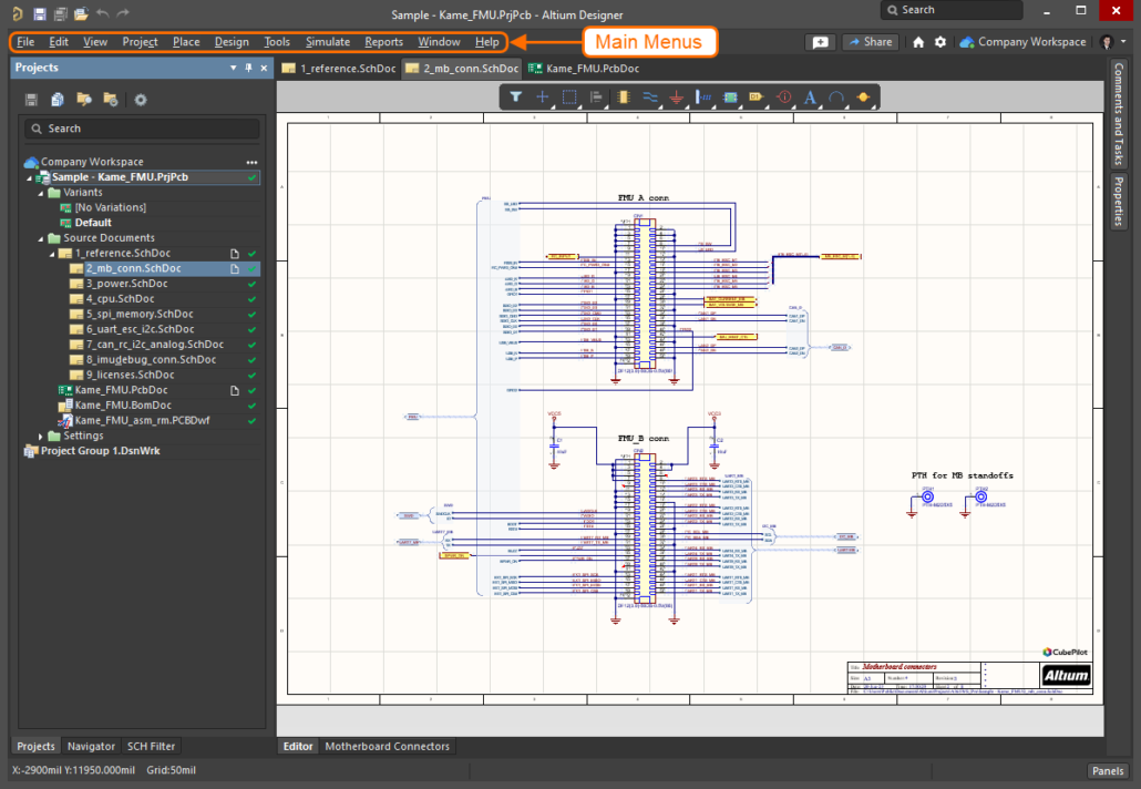
We have rich experience engineer to create a layout using a software platform like Altium Designer. This layout shows you the exact appearance and placement of the components on your board.
One of our Hardware Design Services is small-batch manufacturing, which allows you to test your idea quickly and verify the functionality of the hardware design and PCB board.
1.How does the type of solder mask used affect the PCB’s performance?
We have broad development space in domestic and foreign markets. circuit card assembly vs pcbs have great advantages in terms of price, quality, and delivery date.
The type of solder mask used can affect the PCB’s performance in several ways:
1. Insulation: Solder mask is used to insulate the copper traces on a PCB, preventing them from coming into contact with each other and causing a short circuit. The type of solder mask used can affect the level of insulation provided, which can impact the overall reliability and functionality of the PCB.
2. Solderability: Solder mask also plays a crucial role in the soldering process. The type of solder mask used can affect the surface tension and wetting properties of the solder, which can impact the quality of the solder joints and the overall reliability of the PCB.
3. Thermal resistance: Solder mask can also act as a thermal barrier, protecting the PCB from excessive heat. The type of solder mask used can affect the thermal resistance of the PCB, which can impact its ability to dissipate heat and its overall thermal performance.
4. Chemical resistance: Solder mask is also exposed to various chemicals during the PCB manufacturing process, such as flux and cleaning agents. The type of solder mask used can affect its resistance to these chemicals, which can impact the overall durability and reliability of the PCB.
5. Electrical properties: The type of solder mask used can also affect the electrical properties of the PCB, such as its dielectric constant and dissipation factor. These properties can impact the performance of high-frequency circuits and signal integrity.
Overall, the type of solder mask used can have a significant impact on the performance, reliability, and durability of a PCB. It is essential to carefully select the appropriate solder mask for a specific application to ensure optimal performance.
2.How does the number of layers in a PCB affect its functionality?
We should have a stable supply chain and logistics capabilities, and provide customers with high -quality, low -priced circuit card assembly vs pcb products.
The number of layers in a PCB (Printed Circuit Board) can affect its functionality in several ways:
1. Complexity: The number of layers in a PCB determines the complexity of the circuit design that can be implemented. More layers allow for more components and connections to be included in the design, making it more complex and versatile.
2. Size: A PCB with more layers can be smaller in size compared to a PCB with fewer layers, as it allows for a more compact layout of components and connections. This is especially important in devices with limited space, such as smartphones and wearables.
3. Signal Integrity: The number of layers in a PCB can also affect the signal integrity of the circuit. More layers allow for better routing of signals, reducing the chances of interference and crosstalk between different components.
4. Power Distribution: PCBs with more layers can have dedicated power and ground planes, which help in distributing power evenly across the circuit. This improves the overall performance and stability of the circuit.
5. Cost: The number of layers in a PCB can also affect its cost. More layers mean more materials and manufacturing processes, which can increase the overall cost of the PCB.
6. Thermal Management: PCBs with more layers can have better thermal management, as they allow for the placement of thermal vias and heat sinks to dissipate heat more efficiently. This is important for high-power applications that generate a lot of heat.
In summary, the number of layers in a PCB can significantly impact its functionality, complexity, size, signal integrity, power distribution, cost, and thermal management. Designers must carefully consider the number of layers required for a PCB based on the specific requirements of the circuit and the device it will be used in.
3.Can PCBs have different shapes and sizes?
Our company has many years of circuit card assembly vs pcb experience and expertise.
Yes, PCBs (printed circuit boards) can have different shapes and sizes depending on the specific design and purpose of the circuit. They can range from small and compact to large and complex, and can be rectangular, circular, or even irregularly shaped. The shape and size of a PCB is determined by the layout of the components and the desired functionality of the circuit.
4.What are the different types of through-hole mounting techniques used in PCBs?
We have flexible production capacity. Whether you are large orders or small orders, you can produce and release goods in a timely manner to meet customer needs.
1. Through-Hole Plating: This is the most common through-hole mounting technique, where the holes in the PCB are plated with a conductive material, usually copper, to create a connection between the layers of the board.
2. Through-Hole Soldering: In this technique, the components are inserted into the plated holes and then soldered to the pads on the opposite side of the board. This provides a strong mechanical connection and good electrical conductivity.
3. Through-Hole Riveting: In this method, the components are inserted into the plated holes and then secured with a rivet or pin. This is commonly used for high-power components or in applications where the board may experience high levels of vibration.
4. Through-Hole Press-Fit: This technique involves inserting the component leads into the plated holes and then pressing them into place using a specialized tool. This provides a strong mechanical connection without the need for soldering.
5. Through-Hole Wave Soldering: In this method, the components are inserted into the plated holes and then passed over a wave of molten solder, which creates a strong solder joint between the component leads and the PCB pads.
6. Through-Hole Reflow Soldering: This technique is similar to wave soldering, but instead of passing over a wave of molten solder, the board is heated in a controlled environment to melt the solder and create a strong joint.
7. Through-Hole Hand Soldering: This is a manual method of soldering where the components are inserted into the plated holes and then soldered by hand using a soldering iron. This is commonly used for small-scale production or for repairs.
8. Through-Hole Pin-in-Paste: This technique involves inserting the component leads into the plated holes and then applying solder paste to the holes before reflow soldering. This provides a strong mechanical connection and good solder joints.
9. Through-Hole Pin-in-Hole: In this method, the component leads are inserted into the plated holes and then bent to form a right angle, creating a secure mechanical connection. This is commonly used for components with large leads, such as electrolytic capacitors.
10. Through-Hole Hand Assembly: This is a manual method of assembly where the components are inserted into the plated holes and then secured with hand tools, such as screws or nuts. This is commonly used for large or heavy components that require additional support.
5.Can PCBs be designed to withstand high vibration or shock?
We have established long-term and stable partnerships with our suppliers, so we have great advantages in price and cost and quality assurance.
Yes, PCBs can be designed to withstand high vibration or shock by incorporating certain design features and using appropriate materials. Some ways to make a PCB more resistant to vibration and shock include:
1. Using a thicker and more rigid PCB substrate material, such as FR-4 or ceramic, to provide better structural support and reduce flexing.
2. Adding additional support structures, such as mounting holes or stiffeners, to secure the PCB to the chassis or enclosure.
3. Using smaller and more compact components to reduce the overall weight and size of the PCB, which can help minimize the effects of vibration.
4. Using shock-absorbing materials, such as rubber or foam, between the PCB and the mounting surface to absorb and dampen vibrations.
5. Designing the PCB layout to minimize the length and number of traces and vias, which can reduce the risk of mechanical stress and failure.
6. Using surface mount technology (SMT) components instead of through-hole components, as they are less prone to damage from vibration.
7. Incorporating conformal coating or potting materials to protect the PCB and components from moisture and mechanical stress.
It is important to consider the specific requirements and environment in which the PCB will be used when designing for high vibration or shock resistance. Consulting with a PCB design expert can also help ensure that the PCB is properly designed to withstand these conditions.
MTI is a high-tech company specializing in PCB manufacturing, PCB assembly and parts procurement services with more than 20 years of experience. We are committed to producing various types of printed circuit boards, mainly including single-sided, double-sided, multi-layer circuit boards, high-precision HDI, flexible boards (FPC), rigid-flex boards (including HDI), metal circuit boards and their SMD plugin.Product line application areas include:industrial control.Fast response, strict quality control, best service, and strong technical support export our PCB products to global markets,including,Brunei,Iran,Anguilla,Estonia,Navassa Island,Bhutan.
MTI would like to build long and stable business relationship with the customers from all over the world on the basis of mutual benefits and mutual progress;Choose MTI , Drive you Success!
We keep good quality and competitive price to ensure our customers benefit
Sales country
All over the world for example:Brunei,Iran,Anguilla,Estonia,Navassa Island,Bhutan
One of our Hardware Design Services is small-batch manufacturing, which allows you to test your idea quickly and verify the functionality of the hardware design and PCB board.
We have rich experience engineer to create a layout using a software platform like Altium Designer. This layout shows you the exact appearance and placement of the components on your board.
Your deliverables are always ahead of schedule and of the highest quality.
1.How does the hole size and shape impact the manufacturing process of a PCB?
We continue to invest in research and development and continue to launch innovative products.
The hole size and shape on a PCB can impact the manufacturing process in several ways:
1. Drilling process: The size and shape of the holes determine the type of drill bit and the drilling speed required for creating the holes. Smaller holes require smaller drill bits and slower drilling speeds, while larger holes require larger drill bits and faster drilling speeds. The shape of the hole can also affect the stability of the drill bit and the accuracy of the drilling process.
2. Plating process: After the holes are drilled, they need to be plated with a conductive material to create electrical connections between different layers of the PCB. The size and shape of the holes can affect the plating process, as larger or irregularly shaped holes may require more plating material and longer plating times.
3. Soldering process: The size and shape of the holes can also impact the soldering process. Smaller holes may require more precise placement of components and more careful soldering techniques, while larger holes may allow for easier soldering.
4. Component placement: The size and shape of the holes can also affect the placement of components on the PCB. Smaller holes may limit the size of components that can be used, while larger holes may allow for more flexibility in component placement.
5. PCB design: The size and shape of the holes can also impact the overall design of the PCB. Different hole sizes and shapes may require different routing and layout strategies, which can affect the overall functionality and performance of the PCB.
Overall, the size and shape of the holes on a PCB can significantly impact the manufacturing process and should be carefully considered during the design phase to ensure efficient and accurate production.
2.How does the type of PCB connection (wired or wireless) impact its design and features?
Our products & services cover a wide range of areas and meet the needs of different fields.
The type of PCB connection, whether wired or wireless, can have a significant impact on the design and features of the PCB. Some of the key ways in which the type of connection can impact the PCB design and features are:
1. Size and form factor: Wired PCBs typically require physical connectors and cables, which can add to the overall size and form factor of the PCB. On the other hand, wireless PCBs do not require physical connectors and cables, allowing for a smaller and more compact design.
2. Power consumption: Wired PCBs require a constant supply of power to function, whereas wireless PCBs can operate on battery power. This can impact the power consumption and battery life of the device, which in turn can affect the overall design and features of the PCB.
3. Flexibility and mobility: Wireless PCBs offer greater flexibility and mobility as they do not have physical connections that restrict movement. This can be advantageous in applications where the device needs to be moved or used in different locations.
4. Data transfer speed: Wired PCBs typically have faster data transfer speeds compared to wireless PCBs. This can impact the design and features of the PCB, as certain applications may require high-speed data transfer.
5. Cost: The type of connection can also impact the cost of the PCB. Wired PCBs may require additional components such as connectors and cables, which can add to the overall cost. Wireless PCBs, on the other hand, may require more advanced technology and components, making them more expensive.
6. Reliability: Wired PCBs are generally considered more reliable as they have a physical connection, which is less prone to interference or signal loss. Wireless PCBs, on the other hand, may be more susceptible to interference and signal loss, which can impact their reliability.
Overall, the type of PCB connection can significantly impact the design and features of the PCB, and it is important to carefully consider the specific requirements of the application when choosing between wired and wireless connections.
3.How does the number of layers in a PCB affect its functionality?
We should have a stable supply chain and logistics capabilities, and provide customers with high -quality, low -priced circuit card assembly process products.
The number of layers in a PCB (Printed Circuit Board) can affect its functionality in several ways:
1. Complexity: The number of layers in a PCB determines the complexity of the circuit design that can be implemented. More layers allow for more components and connections to be included in the design, making it more complex and versatile.
2. Size: A PCB with more layers can be smaller in size compared to a PCB with fewer layers, as it allows for a more compact layout of components and connections. This is especially important in devices with limited space, such as smartphones and wearables.
3. Signal Integrity: The number of layers in a PCB can also affect the signal integrity of the circuit. More layers allow for better routing of signals, reducing the chances of interference and crosstalk between different components.
4. Power Distribution: PCBs with more layers can have dedicated power and ground planes, which help in distributing power evenly across the circuit. This improves the overall performance and stability of the circuit.
5. Cost: The number of layers in a PCB can also affect its cost. More layers mean more materials and manufacturing processes, which can increase the overall cost of the PCB.
6. Thermal Management: PCBs with more layers can have better thermal management, as they allow for the placement of thermal vias and heat sinks to dissipate heat more efficiently. This is important for high-power applications that generate a lot of heat.
In summary, the number of layers in a PCB can significantly impact its functionality, complexity, size, signal integrity, power distribution, cost, and thermal management. Designers must carefully consider the number of layers required for a PCB based on the specific requirements of the circuit and the device it will be used in.
4.Can PCBs be customized based on specific design requirements?
We have rich industry experience and professional knowledge, and have strong competitiveness in the market.
Yes, PCBs (printed circuit boards) can be customized based on specific design requirements. This is typically done through the use of computer-aided design (CAD) software, which allows for the creation of a custom layout and design for the PCB. The design can be tailored to meet specific size, shape, and functionality requirements, as well as incorporate specific components and features. The customization process may also involve selecting the appropriate materials and manufacturing techniques to ensure the PCB meets the desired specifications.
5.How important is the trace width and spacing in a PCB design?
Our circuit card assembly process products have competitive and differentiated advantages, and actively promote digital transformation and innovation.
The trace width and spacing in a PCB design are crucial factors that can greatly affect the performance and reliability of the circuit. Here are some reasons why:
1. Current carrying capacity: The trace width determines the amount of current that can flow through the trace without causing excessive heating. If the trace width is too narrow, it can lead to overheating and damage to the circuit.
2. Voltage drop: The trace width also affects the voltage drop across the trace. A narrow trace will have a higher resistance, resulting in a higher voltage drop. This can cause a decrease in the voltage level at the end of the trace, affecting the performance of the circuit.
3. Signal integrity: The spacing between traces is critical for maintaining signal integrity. If the spacing is too narrow, it can lead to crosstalk and interference between signals, resulting in errors and malfunctions in the circuit.
4. Thermal management: The spacing between traces also plays a role in thermal management. Adequate spacing between traces allows for better air circulation, which helps dissipate heat from the circuit. This is especially important for high-power circuits.
5. Manufacturing constraints: The trace width and spacing also need to be considered in the manufacturing process. If the traces are too close together, it can be challenging to etch and inspect the PCB, leading to manufacturing defects.
In summary, the trace width and spacing are critical parameters that need to be carefully considered in PCB design to ensure proper functioning and reliability of the circuit.
6.How does the type of solder mask used affect the PCB’s performance?
We have broad development space in domestic and foreign markets. circuit card assembly processs have great advantages in terms of price, quality, and delivery date.
The type of solder mask used can affect the PCB’s performance in several ways:
1. Insulation: Solder mask is used to insulate the copper traces on a PCB, preventing them from coming into contact with each other and causing a short circuit. The type of solder mask used can affect the level of insulation provided, which can impact the overall reliability and functionality of the PCB.
2. Solderability: Solder mask also plays a crucial role in the soldering process. The type of solder mask used can affect the surface tension and wetting properties of the solder, which can impact the quality of the solder joints and the overall reliability of the PCB.
3. Thermal resistance: Solder mask can also act as a thermal barrier, protecting the PCB from excessive heat. The type of solder mask used can affect the thermal resistance of the PCB, which can impact its ability to dissipate heat and its overall thermal performance.
4. Chemical resistance: Solder mask is also exposed to various chemicals during the PCB manufacturing process, such as flux and cleaning agents. The type of solder mask used can affect its resistance to these chemicals, which can impact the overall durability and reliability of the PCB.
5. Electrical properties: The type of solder mask used can also affect the electrical properties of the PCB, such as its dielectric constant and dissipation factor. These properties can impact the performance of high-frequency circuits and signal integrity.
Overall, the type of solder mask used can have a significant impact on the performance, reliability, and durability of a PCB. It is essential to carefully select the appropriate solder mask for a specific application to ensure optimal performance.
7.Is it possible to have different components on each side of a PCB?
We focus on innovation and continuous improvement to maintain a competitive advantage.
Yes, it is possible to have different components on each side of a PCB. This is known as a double-sided PCB or a two-layer PCB. The components on each side can be connected through vias, which are small holes drilled through the PCB that allow for electrical connections between the layers. This allows for more compact and complex circuit designs. However, it also adds complexity to the manufacturing process and may increase the cost of the PCB.
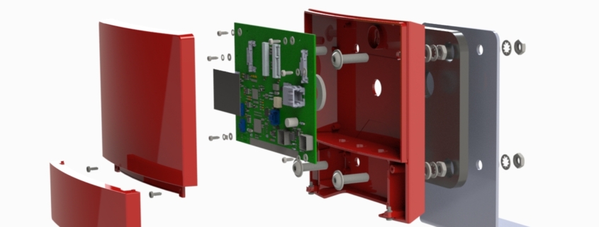
The ESP32 module, renowned for its versatility and power, has become a staple in IoT projects. Integrating this module into custom PCB designs requires precision and expertise. MTI, a leading PCB assembly manufacturer, excels in creating high-quality PCBs tailored for ESP32 integration. This guide explores the benefits and methods of incorporating the ESP32 module into custom PCBs, showcasing MTI’s capabilities and the advantages they offer.
Advanced Manufacturing Techniques
MTI employs state-of-the-art manufacturing techniques to ensure high-quality PCB designs that seamlessly integrate with the ESP32 module.
Precision Engineering
MTI utilizes advanced CNC machinery and precise engineering processes to create PCBs with exact specifications. This precision is crucial for the proper functioning of the ESP32 module, ensuring reliable and efficient performance in various applications.
High-Quality Materials
The PCBs are crafted from high-quality materials sourced from reputable suppliers. These materials guarantee durability and performance, essential for supporting the capabilities of the ESP32 module in IoT projects.
Customization and Flexibility
MTI offers extensive customization options through its OEM/ODM services, allowing for tailored PCB design that meet specific project requirements.
Tailored PCB Designs
Clients can specify their exact needs for PCB designs to optimize the integration of the ESP32 module. MTI’s R&D team works closely with clients to develop custom solutions that align with their unique project goals and technical requirements.
Flexible Manufacturing Solutions
MTI’s flexible manufacturing solutions cater to both small and large production runs, providing scalability without compromising quality. This adaptability ensures that clients receive high-quality PCBs regardless of the order size.
Integration Benefits
Integrating the ESP32 module into custom PCB designs offers several benefits, enhancing the overall performance and functionality of IoT projects.
Enhanced Performance
Custom PCB designs optimized for the ESP32 module enhance overall system performance. The precise layout and connections ensure that the module operates at its full potential, delivering reliable and efficient performance.
Reduced Development Time
MTI’s expertise in PCB design and manufacturing helps reduce development time. By leveraging their advanced capabilities, clients can quickly iterate and refine their designs, speeding up the time-to-market for their products.
Quality Control and Assurance
MTI places a strong emphasis on quality control to ensure that every PCB meets stringent standards of excellence.
Comprehensive Testing
Each PCB undergoes comprehensive testing to verify its performance, durability, and functionality. This rigorous quality control process ensures that clients receive reliable and high-performing PCBs.
Consistent Quality Standards
MTI maintains consistent quality standards across all products. From raw material selection to final assembly, every step of the manufacturing process is closely monitored to ensure optimal quality and performance.
Cost Performance Benefits
MTI’s efficient manufacturing processes and strategic sourcing result in significant cost performance benefits, making them a smart choice for PCB production.
Competitive Pricing
MTI offers competitive pricing without compromising on quality, leveraging their scale and efficient processes. This cost advantage provides excellent value for clients, enhancing their overall cost performance.
Economies of Scale
By achieving economies of scale, MTI reduces production costs, passing these savings on to clients. This approach ensures high-quality PCBs at affordable prices, making advanced ESP32 module integration accessible to a broader market.
Supply Chain Efficiency
MTI’s well-established supply chain ensures timely delivery and consistent quality, enhancing their competitive edge in the market.
Reliable Supplier Network
MTI has built a reliable supplier network that ensures the consistent availability of high-quality materials. This network supports uninterrupted production and timely order fulfillment, reinforcing MTI’s reputation as a dependable manufacturer.
Global Distribution Capabilities
MTI’s global distribution capabilities ensure that clients receive their PCBs promptly, regardless of their location. This global reach enhances client satisfaction and supports the company’s growth in international markets.
Conclusion
MTI’s expertise in integrating the ESP32 module into custom PCB designs combines advanced manufacturing techniques, extensive customization options, and rigorous quality control to deliver high-quality solutions. As a leading PCB assembly manufacturer in China, MTI offers competitive pricing, efficient supply chain management, and superior cost performance.
In the competitive electronics industry, achieving economies of scale in PCB production is crucial for reducing costs and increasing efficiency. MTI, a leading PCB assembly manufacturer, leverages advanced manufacturing techniques and strategic planning to deliver cost-effective solutions without compromising on quality. This article explores the methods and benefits of achieving economies of scale in PCB production, highlighting MTI’s capabilities and advantages.
Advanced Manufacturing Techniques
MTI employs cutting-edge manufacturing techniques to maximize efficiency and achieve economies of scale.
High-Volume Production
MTI’s factory is equipped with state-of-the-art machinery capable of high-volume production. This capacity allows for the efficient manufacturing of large quantities of PCBs, reducing per-unit costs and optimizing resource utilization.
Automation and Robotics
The integration of automation and robotics in MTI’s manufacturing process enhances precision and speed. Automated systems streamline production workflows, minimize human error, and increase output, contributing significantly to economies of scale.
Strategic Sourcing and Supply Chain Management
Effective sourcing and supply chain management are essential components of achieving economies of scale.
Bulk Material Sourcing
MTI sources materials in bulk from reliable suppliers, ensuring consistent quality while benefiting from volume discounts. This strategic approach reduces material costs and enhances cost performance, providing a competitive advantage.
Efficient Logistics and Distribution
MTI maintains an efficient logistics network that ensures timely delivery of materials and finished products. By optimizing transportation and inventory management, the company minimizes delays and reduces overhead costs.
Customization and Flexibility
MTI offers extensive customization options through its OEM/ODM services, catering to diverse client needs while maintaining cost efficiency.
Tailored PCB Designs
Clients can request tailored PCB designs to meet their specific requirements. MTI’s R&D team collaborates closely with clients to develop custom solutions that align with their project goals, ensuring optimal performance and cost efficiency.
Scalable Production Solutions
MTI’s scalable production solutions accommodate both small and large orders, providing flexibility without sacrificing economies of scale. This adaptability ensures that clients receive high-quality PCBs regardless of order size.
Quality Control and Assurance
Maintaining high-quality standards is crucial for achieving economies of scale without compromising product integrity.
Rigorous Testing Procedures
Every PCB undergoes rigorous testing procedures to ensure it meets stringent quality standards. This comprehensive quality control process minimizes defects and reduces the need for costly rework, enhancing overall cost performance.
Consistent Quality Standards
MTI adheres to consistent quality standards across all production stages. From material selection to final assembly, each step is meticulously monitored to ensure the highest level of quality and reliability.
Cost Performance Benefits
Achieving economies of scale in PCB production provides significant cost performance benefits, making MTI a preferred choice for clients worldwide.
Reduced Production Costs
High-volume production and strategic sourcing reduce overall production costs, enabling MTI to offer competitive pricing. This cost advantage allows clients to maximize their investment and achieve better profitability.
Enhanced Efficiency
Automation, bulk sourcing, and efficient logistics contribute to enhanced production efficiency. This efficiency translates to faster turnaround times, lower operational costs, and improved client satisfaction.
Supply Chain Efficiency
MTI’s well-established supply chain ensures the seamless delivery of products, enhancing their competitive edge in the market.
Reliable Supplier Network
MTI has built a reliable supplier network that ensures the consistent availability of high-quality materials. This network supports uninterrupted production and timely order fulfillment, reinforcing MTI’s reputation as a dependable manufacturer.
Global Distribution Capabilities
MTI’s global distribution capabilities ensure that clients receive their PCBs promptly, regardless of their location. This global reach enhances client satisfaction and supports the company’s growth in international markets.
Conclusion
MTI’s approach to achieving economies of scale in PCB production combines advanced manufacturing techniques, strategic sourcing, and rigorous quality control to deliver cost-effective and high-quality solutions. As a leading PCB assembly manufacturer in China, MTI offers extensive customization options, competitive pricing, and efficient supply chain management.
https://www.mintecinno.com/wp-content/uploads/2023/08/embedded-system-1-mechanical-exploded-view.webp.jpg7511223mtipcbahttps://www.mintecinno.com/wp-content/uploads/2025/02/MTI-PCBA-长方形.pngmtipcba2024-06-22 07:38:132024-06-22 07:38:13Achieving Economies of Scale in PCB Production
In the fast-paced world of electronics, having a reliable PCB prototype is crucial for new product development. MTI, a renowned PCB manufacturer, offers high-quality PCB prototypes that cater to the diverse needs of innovators and developers. This article delves into the features, benefits, and advantages of MTI’s PCB prototype, showcasing their commitment to excellence in manufacturing, design, and cost performance.
Advanced Manufacturing Techniques
MTI employs state-of-the-art manufacturing techniques to produce top-tier PCB prototypes that meet the stringent requirements of new product development.
Precision Engineering
MTI’s PCB prototypes are crafted with precision engineering. Utilizing advanced CNC machinery and cutting-edge technology, the manufacturing process ensures accurate dimensions and consistent quality, resulting in reliable and high-performing prototypes.
High-Quality Materials
The PCB prototypes are constructed using high-quality materials chosen for their durability and performance. These materials are sourced from reputable suppliers, ensuring that each prototype meets the highest standards of quality and reliability.
Customization and Flexibility
MTI offers extensive customization options to meet the specific needs of clients, making their PCB prototypes suitable for a wide range of applications.
Tailored Design Options
Clients can choose from various design options to tailor the PCB prototypes to their unique requirements. Whether it’s adjusting the size, layout, or functionality, MTI’s R&D team collaborates closely with clients to develop custom solutions.
OEM/ODM Services
As an experienced manufacturer, MTI provides comprehensive OEM/ODM services. This allows clients to leverage their expertise in design and manufacturing to create bespoke PCB prototypes that align with their specific project needs.
Efficiency and Performance
MTI’s PCB prototypes are designed to optimize new product development processes, enhancing overall efficiency and performance.
Rapid Prototyping
The advanced manufacturing capabilities at MTI enable rapid prototyping, allowing clients to quickly iterate and refine their designs. This speed is crucial for meeting tight development timelines and bringing new products to market faster.
Reliable Performance
MTI’s PCB prototypes are engineered for reliable performance, ensuring that they function as intended during testing and development. This reliability reduces the risk of errors and enhances the overall quality of the final product.
Quality Control and Assurance
MTI places a strong emphasis on quality control to ensure that every PCB prototype meets rigorous standards of excellence.
Comprehensive Testing
Each PCB prototype undergoes comprehensive testing to verify its performance, durability, and functionality. This thorough quality control process ensures that clients receive prototypes that are both reliable and high-performing.
Consistent Standards
MTI maintains consistent quality standards across all their products. From raw material selection to final assembly, every step of the manufacturing process is closely monitored to ensure optimal quality and performance.
Cost Performance Benefits
Investing in MTI’s PCB prototypes offers significant cost performance benefits, making them a smart choice for businesses seeking efficient new product development solutions.
Reduced Development Costs
The efficiency and reliability of the PCB prototypes reduce development costs by minimizing the need for multiple iterations and reworks. This enhances overall cost performance, providing excellent value for investment.
Competitive Pricing
As a leading manufacturer in China, MTI leverages economies of scale to offer competitive pricing without compromising on quality. This makes their PCB prototypes an affordable and attractive option for clients worldwide.
Supply Chain Efficiency
MTI’s well-established supply chain ensures timely delivery and consistent quality, enhancing their competitive edge in the market.
Efficient Logistics
The company’s efficient logistics network enables prompt and reliable delivery of products to clients globally. This ensures that clients receive their PCB prototypes on schedule, facilitating smooth development processes.
Reliable Distribution Network
MTI has a robust distribution network that ensures the availability of their products in key markets. This reliability helps maintain client satisfaction and fosters long-term partnerships.
Conclusion
MTI’s reliable PCB prototypes combine advanced manufacturing techniques, customization options, and high-performance features to deliver efficient new product development solutions. With a focus on quality control, cost performance, and supply chain efficiency, MTI stands out as a leading manufacturer in China. Their commitment to excellence ensures that clients receive top-tier PCB prototypes that meet their specific needs and drive innovation.
https://www.mintecinno.com/wp-content/uploads/2023/08/Manufacturing.jpg8001200mtipcbahttps://www.mintecinno.com/wp-content/uploads/2025/02/MTI-PCBA-长方形.pngmtipcba2024-06-22 07:31:572024-06-22 07:31:57Reliable PCB Prototype for New Product Development
MTI is a manufacturer of high-precision printed circuit board (PCB).We specialize in the manufacture of high precision double-sided and multilayer printed circuit boards, We provide high quality products and faster service for high-tech companies.
We have a group of experienced staff and high-quality management team, set up a complete quality assurance system. Products include FR-4 PCB, Metal PCB and RFPCB (ceramic PCB, PTFE PCB), circuit card assembly manufacturing process, etc. Have rich experience in the production of thick copper PCB, RF PCB, high Tg PCB, HDI PCB.With ISO9001, ISO14001, TS16949, ISO 13485, RoHS certifications.
We keep good quality and competitive price to ensure our customers benefit
Sales country
All over the world for example:Belarus,Suriname,Guam,Peru,Spratly Islands
Your deliverables are always ahead of schedule and of the highest quality.
One of our Hardware Design Services is small-batch manufacturing, which allows you to test your idea quickly and verify the functionality of the hardware design and circuit card assembly manufacturing process.
We have rich experience engineer to create a layout using a software platform like Altium Designer. This layout shows you the exact appearance and placement of the components on your board.
1.How does the type of PCB finish affect its durability and lifespan?
I have a comprehensive after -sales service system, which can pay attention to market trends in time and adjust our strategy in a timely manner.
The type of PCB finish can have a significant impact on the durability and lifespan of a PCB. The finish is the final coating applied to the surface of the PCB to protect it from environmental factors and ensure proper functionality. Some common types of PCB finishes include HASL (Hot Air Solder Leveling), ENIG (Electroless Nickel Immersion Gold), and OSP (Organic Solderability Preservative).
1. HASL (Hot Air Solder Leveling):
HASL is a popular and cost-effective finish that involves coating the PCB with a layer of molten solder and then leveling it with hot air. This finish provides good solderability and is suitable for most applications. However, it is not very durable and can be prone to oxidation, which can affect the performance of the PCB over time. HASL finish also has a limited shelf life and may require rework after a certain period.
2. ENIG (Electroless Nickel Immersion Gold):
ENIG is a more advanced and durable finish compared to HASL. It involves depositing a layer of nickel and then a layer of gold on the surface of the PCB. This finish provides excellent corrosion resistance and is suitable for high-reliability applications. ENIG finish also has a longer shelf life and does not require rework as frequently as HASL.
3. OSP (Organic Solderability Preservative):
OSP is a thin organic coating applied to the surface of the PCB to protect it from oxidation. It is a cost-effective finish and provides good solderability. However, OSP finish is not as durable as ENIG and may require rework after a certain period. It is also not suitable for high-temperature applications.
In summary, the type of PCB finish can affect its durability and lifespan in the following ways:
– Corrosion resistance: Finishes like ENIG and OSP provide better corrosion resistance compared to HASL, which can affect the performance and lifespan of the PCB.
– Shelf life: Finishes like ENIG have a longer shelf life compared to HASL, which may require rework after a certain period.
– Solderability: All finishes provide good solderability, but ENIG and OSP are more suitable for high-reliability applications.
– Environmental factors: The type of finish can also affect the PCB’s resistance to environmental factors like humidity, temperature, and chemicals, which can impact its durability and lifespan.
In conclusion, choosing the right type of PCB finish is crucial for ensuring the durability and longevity of the PCB. Factors such as the application, environmental conditions, and budget should be considered when selecting the appropriate finish for a PCB.
2.Can PCBs be customized based on specific design requirements?
We have rich industry experience and professional knowledge, and have strong competitiveness in the market.
Yes, PCBs (printed circuit boards) can be customized based on specific design requirements. This is typically done through the use of computer-aided design (CAD) software, which allows for the creation of a custom layout and design for the PCB. The design can be tailored to meet specific size, shape, and functionality requirements, as well as incorporate specific components and features. The customization process may also involve selecting the appropriate materials and manufacturing techniques to ensure the PCB meets the desired specifications.
3.What is the minimum distance required between components on a PCB?
We have advanced production equipment and technology to meet the needs of customers, and can provide customers with high quality, low priced circuit card assembly manufacturing process products.
The minimum distance required between components on a PCB depends on various factors such as the type of components, their size, and the manufacturing process used. Generally, the minimum distance between components is determined by the manufacturer’s design rules and guidelines.
For surface mount components, the minimum distance between components is typically 0.2mm to 0.3mm. This distance is necessary to ensure that the solder paste does not bridge between the pads during the reflow process.
For through-hole components, the minimum distance between components is typically 1mm to 2mm. This distance is necessary to ensure that the components do not interfere with each other during the assembly process.
In high-speed and high-frequency applications, the minimum distance between components may need to be increased to avoid signal interference and crosstalk. In these cases, the manufacturer’s design rules and guidelines should be followed closely.
Overall, the minimum distance between components on a PCB should be determined based on the specific requirements of the design and the capabilities of the manufacturing process.
4.What are the advantages and disadvantages of using a rigid or flexible PCB?
We have the leading technology and innovation capabilities, and attach importance to employee training and development, and provide promotion opportunities.
Advantages of rigid PCB:
1. Durability: Rigid PCBs are more durable and can withstand higher levels of stress and strain compared to flexible PCBs.
2. Better for high-speed applications: Rigid PCBs are better suited for high-speed applications as they have better signal integrity and lower signal loss.
3. Cost-effective: Rigid PCBs are generally less expensive to manufacture compared to flexible PCBs.
4. Easier to assemble: Rigid PCBs are easier to assemble and can be used with automated assembly processes, making them more efficient for mass production.
5. Higher component density: Rigid PCBs can accommodate a higher number of components and have a higher component density compared to flexible PCBs.
Disadvantages of rigid PCB:
1. Limited flexibility: Rigid PCBs are not flexible and cannot be bent or twisted, making them unsuitable for certain applications.
2. Bulkier: Rigid PCBs are bulkier and take up more space compared to flexible PCBs, which can be a disadvantage in compact electronic devices.
3. Prone to damage: Rigid PCBs are more prone to damage from vibrations and shocks, which can affect their performance.
Advantages of flexible PCB:
1. Flexibility: Flexible PCBs can be bent, twisted, and folded, making them suitable for applications where space is limited or where the PCB needs to conform to a specific shape.
2. Lightweight: Flexible PCBs are lightweight and take up less space compared to rigid PCBs, making them ideal for portable electronic devices.
3. Better for high vibration environments: Flexible PCBs are more resistant to vibrations and shocks, making them suitable for use in high vibration environments.
4. Higher reliability: Flexible PCBs have fewer interconnects and solder joints, reducing the chances of failure and increasing reliability.
Disadvantages of flexible PCB:
1. Higher cost: Flexible PCBs are generally more expensive to manufacture compared to rigid PCBs.
2. Limited component density: Flexible PCBs have a lower component density compared to rigid PCBs, which can limit their use in high-density applications.
3. Difficult to repair: Flexible PCBs are more difficult to repair compared to rigid PCBs, as they require specialized equipment and expertise.
4. Less suitable for high-speed applications: Flexible PCBs have higher signal loss and lower signal integrity compared to rigid PCBs, making them less suitable for high-speed applications.
5.What materials are commonly used to make PCBs?
We have advantages in marketing and channel expansion. Suppliers have established good cooperative relations, continuously improved workflows, improved efficiency and productivity, and provided customers with high -quality products and services.
1. Copper: Copper is the most commonly used material for PCBs. It is used as the conductive layer for the circuit traces and pads.
2. FR4: FR4 is a type of fiberglass-reinforced epoxy laminate that is used as the base material for most PCBs. It provides good mechanical strength and insulation properties.
3. Solder mask: Solder mask is a layer of polymer that is applied over the copper traces to protect them from oxidation and to prevent solder bridges during assembly.
4. Silkscreen: Silkscreen is a layer of ink that is printed on top of the solder mask to provide component labels, reference designators, and other information.
5. Tin/lead or lead-free solder: Solder is used to attach components to the PCB and to create electrical connections between them.
6. Gold: Gold is used for plating the contact pads and vias on the PCB, as it provides good conductivity and corrosion resistance.
7. Silver: Silver is sometimes used as an alternative to gold for plating contact pads and vias, as it is cheaper but still provides good conductivity.
8. Nickel: Nickel is used as a barrier layer between the copper and gold or silver plating to prevent them from diffusing into each other.
9. Epoxy resin: Epoxy resin is used as an adhesive to bond the layers of the PCB together.
10. Ceramic: Ceramic materials are used for specialized PCBs that require high thermal conductivity and insulation properties, such as in high-power applications.
MTI specializes in turn-key electronics manufacturing manufacturing service, providing comprehensive solutions from product documentation to high-quality product delivery worldwide.
With a wide range, good quality, reasonable prices and stylish designs, our products are extensively used in medical.Our products are widely recognized and trusted by users and can meet continuously changing economic and social needs.We welcome new and old customers from all walks of life to contact us for future business relationships and mutual success!
We keep good quality and competitive price to ensure our customers benefit
Sales country
All over the world for example:Martinique,United States of America,Guinea,Nepal,Haiti,Latvia,Suriname,Mauritius
Your deliverables are always ahead of schedule and of the highest quality.
One of our Hardware Design Services is small-batch manufacturing, which allows you to test your idea quickly and verify the functionality of the hardware design and PCB board.
We have rich experience engineer to create a layout using a software platform like Altium Designer. This layout shows you the exact appearance and placement of the components on your board.
1.How does the hole size and shape impact the manufacturing process of a PCB?
We continue to invest in research and development and continue to launch innovative products.
The hole size and shape on a PCB can impact the manufacturing process in several ways:
1. Drilling process: The size and shape of the holes determine the type of drill bit and the drilling speed required for creating the holes. Smaller holes require smaller drill bits and slower drilling speeds, while larger holes require larger drill bits and faster drilling speeds. The shape of the hole can also affect the stability of the drill bit and the accuracy of the drilling process.
2. Plating process: After the holes are drilled, they need to be plated with a conductive material to create electrical connections between different layers of the PCB. The size and shape of the holes can affect the plating process, as larger or irregularly shaped holes may require more plating material and longer plating times.
3. Soldering process: The size and shape of the holes can also impact the soldering process. Smaller holes may require more precise placement of components and more careful soldering techniques, while larger holes may allow for easier soldering.
4. Component placement: The size and shape of the holes can also affect the placement of components on the PCB. Smaller holes may limit the size of components that can be used, while larger holes may allow for more flexibility in component placement.
5. PCB design: The size and shape of the holes can also impact the overall design of the PCB. Different hole sizes and shapes may require different routing and layout strategies, which can affect the overall functionality and performance of the PCB.
Overall, the size and shape of the holes on a PCB can significantly impact the manufacturing process and should be carefully considered during the design phase to ensure efficient and accurate production.
2.What are the differences between a prototype and production PCB?
We have a good reputation and image in the industry. The quality and price advantage of circuit card assemblies products is an important factor in our hard overseas market.
1. Purpose: The main difference between a prototype and production PCB is their purpose. A prototype PCB is used for testing and validation of a design, while a production PCB is used for mass production and commercial use.
2. Design: Prototype PCBs are usually hand-soldered and have a simpler design compared to production PCBs. Production PCBs are designed with more precision and complexity to meet the specific requirements of the final product.
3. Materials: Prototype PCBs are often made with cheaper materials such as FR-4, while production PCBs use higher quality materials such as ceramic or metal core for better performance and durability.
4. Quantity: Prototype PCBs are usually made in small quantities, while production PCBs are manufactured in large quantities to meet the demand of the market.
5. Cost: Due to the use of cheaper materials and smaller quantities, prototype PCBs are less expensive compared to production PCBs. Production PCBs require a larger investment due to the use of higher quality materials and larger quantities.
6. Lead time: Prototype PCBs have a shorter lead time as they are made in smaller quantities and can be hand-soldered. Production PCBs have a longer lead time as they require more complex manufacturing processes and larger quantities.
7. Testing: Prototype PCBs are extensively tested to ensure the design is functional and meets the required specifications. Production PCBs also undergo testing, but the focus is more on quality control and consistency in mass production.
8. Documentation: Prototype PCBs may not have detailed documentation as they are often hand-soldered and used for testing purposes. Production PCBs have detailed documentation to ensure consistency in manufacturing and for future reference.
9. Modifications: Prototype PCBs are easier to modify and make changes to, as they are not mass-produced. Production PCBs are more difficult to modify as any changes can affect the entire production process.
10. Reliability: Production PCBs are designed and manufactured to be more reliable and durable, as they will be used in the final product. Prototype PCBs may not have the same level of reliability as they are used for testing and may not undergo the same level of quality control.
3.What are the advantages and disadvantages of using a rigid or flexible PCB?
We have the leading technology and innovation capabilities, and attach importance to employee training and development, and provide promotion opportunities.
Advantages of rigid PCB:
1. Durability: Rigid PCBs are more durable and can withstand higher levels of stress and strain compared to flexible PCBs.
2. Better for high-speed applications: Rigid PCBs are better suited for high-speed applications as they have better signal integrity and lower signal loss.
3. Cost-effective: Rigid PCBs are generally less expensive to manufacture compared to flexible PCBs.
4. Easier to assemble: Rigid PCBs are easier to assemble and can be used with automated assembly processes, making them more efficient for mass production.
5. Higher component density: Rigid PCBs can accommodate a higher number of components and have a higher component density compared to flexible PCBs.
Disadvantages of rigid PCB:
1. Limited flexibility: Rigid PCBs are not flexible and cannot be bent or twisted, making them unsuitable for certain applications.
2. Bulkier: Rigid PCBs are bulkier and take up more space compared to flexible PCBs, which can be a disadvantage in compact electronic devices.
3. Prone to damage: Rigid PCBs are more prone to damage from vibrations and shocks, which can affect their performance.
Advantages of flexible PCB:
1. Flexibility: Flexible PCBs can be bent, twisted, and folded, making them suitable for applications where space is limited or where the PCB needs to conform to a specific shape.
2. Lightweight: Flexible PCBs are lightweight and take up less space compared to rigid PCBs, making them ideal for portable electronic devices.
3. Better for high vibration environments: Flexible PCBs are more resistant to vibrations and shocks, making them suitable for use in high vibration environments.
4. Higher reliability: Flexible PCBs have fewer interconnects and solder joints, reducing the chances of failure and increasing reliability.
Disadvantages of flexible PCB:
1. Higher cost: Flexible PCBs are generally more expensive to manufacture compared to rigid PCBs.
2. Limited component density: Flexible PCBs have a lower component density compared to rigid PCBs, which can limit their use in high-density applications.
3. Difficult to repair: Flexible PCBs are more difficult to repair compared to rigid PCBs, as they require specialized equipment and expertise.
4. Less suitable for high-speed applications: Flexible PCBs have higher signal loss and lower signal integrity compared to rigid PCBs, making them less suitable for high-speed applications.
4.What are the factors to consider when choosing the right PCB material for a specific application?
We are centered on customers and always pay attention to customers’ needs for circuit card assemblies products.
1. Electrical properties: The electrical properties of the PCB material, such as dielectric constant, loss tangent, and insulation resistance, should be carefully considered to ensure optimal performance for the specific application.
2. Thermal properties: The thermal conductivity and coefficient of thermal expansion of the PCB material are important factors to consider, especially for applications that require high power or operate in extreme temperatures.
3. Mechanical properties: The mechanical strength, stiffness, and flexibility of the PCB material should be evaluated to ensure it can withstand the physical stresses and strains of the application.
4. Chemical resistance: The PCB material should be resistant to any chemicals or solvents that it may come into contact with during its use.
5. Cost: The cost of the PCB material should be considered, as it can vary significantly depending on the type and quality of the material.
6. Availability: Some PCB materials may be more readily available than others, which can affect production timelines and costs.
7. Manufacturing process: The chosen PCB material should be compatible with the manufacturing process, such as etching, drilling, and plating, to ensure efficient and reliable production.
8. Environmental factors: The application environment, such as humidity, moisture, and exposure to UV light, should be taken into account when selecting a PCB material to ensure it can withstand these conditions.
9. Signal integrity: For high-frequency applications, the PCB material should have low signal loss and good signal integrity to prevent interference and ensure accurate signal transmission.
10. RoHS compliance: If the application requires compliance with environmental regulations, such as the Restriction of Hazardous Substances (RoHS) directive, the PCB material should be chosen accordingly.
5.Can PCBs be customized based on specific design requirements?
We have rich industry experience and professional knowledge, and have strong competitiveness in the market.
Yes, PCBs (printed circuit boards) can be customized based on specific design requirements. This is typically done through the use of computer-aided design (CAD) software, which allows for the creation of a custom layout and design for the PCB. The design can be tailored to meet specific size, shape, and functionality requirements, as well as incorporate specific components and features. The customization process may also involve selecting the appropriate materials and manufacturing techniques to ensure the PCB meets the desired specifications.
6.How does the type of vias used affect the performance of a PCB?
Being one of the top circuit card assemblies manufacturers in China, We attach great importance to this detail.
The type of vias used can affect the performance of a PCB in several ways:
1. Signal Integrity: Vias can act as discontinuities in the signal path, causing reflections and signal degradation. The type of via used can impact the impedance and signal integrity of the PCB. For high-speed signals, it is important to use controlled impedance vias to maintain signal integrity.
2. Electrical Performance: The type of via used can also affect the electrical performance of the PCB. For example, through-hole vias have lower resistance and inductance compared to blind or buried vias, which can affect the power delivery and signal transmission on the PCB.
3. Thermal Performance: Vias can also play a role in the thermal performance of a PCB. Through-hole vias can act as thermal vias, allowing heat to dissipate from one layer to another. Blind and buried vias, on the other hand, can trap heat and affect the overall thermal management of the PCB.
4. Manufacturing Cost: The type of via used can also impact the cost of manufacturing the PCB. Blind and buried vias require more complex and expensive processes, while through-hole vias are relatively simpler and cheaper to manufacture.
5. PCB Size and Density: The type of via used can also affect the size and density of the PCB. Blind and buried vias take up less space on the surface of the PCB, allowing for higher density designs. This can be beneficial for smaller and more compact PCBs.
Overall, the type of vias used can have a significant impact on the performance, cost, and design of a PCB. It is important to carefully consider the type of vias needed for a specific application to ensure optimal performance and functionality of the PCB.
7.Can PCBs have different shapes and sizes?
Our company has many years of circuit card assemblies experience and expertise.
Yes, PCBs (printed circuit boards) can have different shapes and sizes depending on the specific design and purpose of the circuit. They can range from small and compact to large and complex, and can be rectangular, circular, or even irregularly shaped. The shape and size of a PCB is determined by the layout of the components and the desired functionality of the circuit.