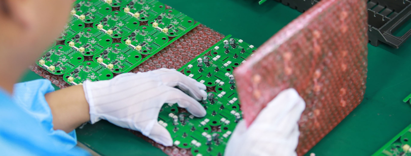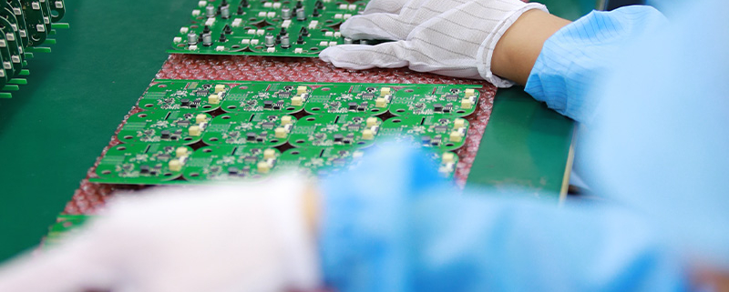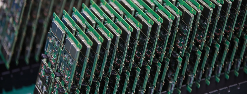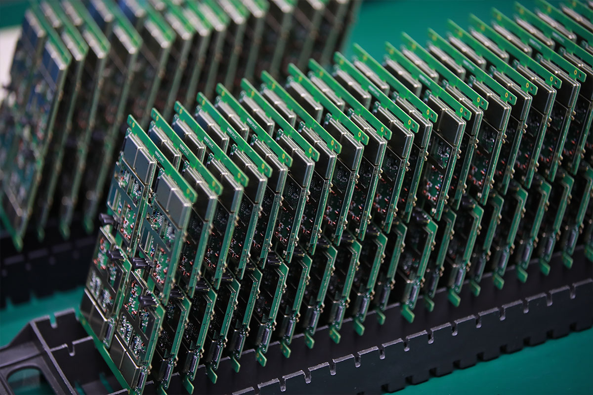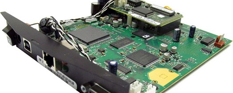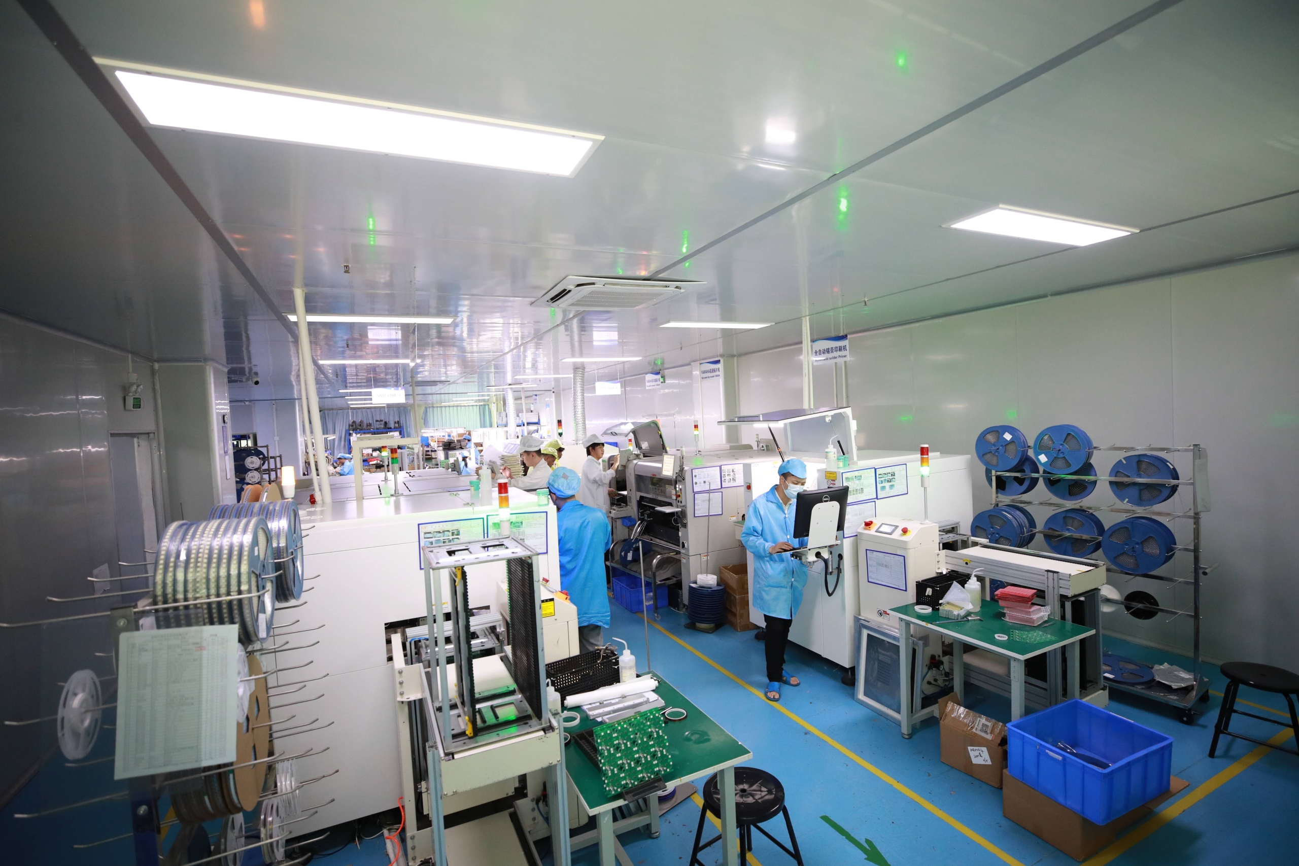
MTI specializes in turn-key electronics manufacturing manufacturing service, providing comprehensive solutions from product documentation to high-quality Circuit Board Assemblies product delivery worldwide.
With a wide range, good quality, reasonable prices and stylish designs, our products are extensively used in computer applications.Our products are widely recognized and trusted by users and can meet continuously changing economic and social needs.We welcome new and old customers from all walks of life to contact us for future business relationships and mutual success!
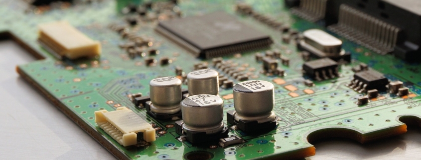
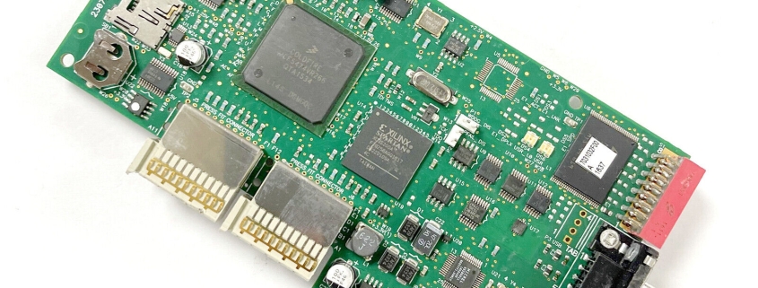
| Product name | circuit board assemblies |
| Keyword | 10 layer pcb stackup,120 mm pcb,printed circuit board assembly manufacturer |
| Place of Origin | China |
| Board Thickness | 2~3.2mm |
| Applicable Industries | computer applications, etc. |
| Service | OEM/ODM manufacturing |
| Certificate | ISO-9001:2015, ISO-14001:2015,ISO-13485:2012.UL/CSA |
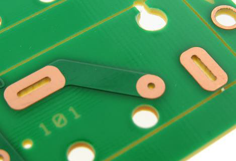
| Solder Mask Color | Red |
| Advantage | We keep good quality and competitive price to ensure our customers benefit |
| Sales country | All over the world for example:Saudi Arabia,Monaco,Serbia and Montenegro,Macedonia,Cambodia |
One of our Hardware Design Services is small-batch manufacturing, which allows you to test your idea quickly and verify the functionality of the hardware design and PCB board.

Your deliverables are always ahead of schedule and of the highest quality.

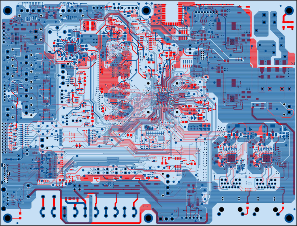
We have rich experience engineer to create a layout using a software platform like Altium Designer. This layout shows you the exact appearance and placement of the components on your board.

FAQs Guide
2.Can PCBs have multiple power planes?
3.How does the hole size and shape impact the manufacturing process of a PCB?
4.Can PCBs be customized based on specific design requirements?
5.How do PCBs handle overcurrent and short circuits?
6.How does the type of vias used affect the performance of a PCB?
7.How important is the trace width and spacing in a PCB design?
8.How does the type of PCB finish affect its durability and lifespan?
1.What are the differences between a prototype and production PCB?
We have a good reputation and image in the industry. The quality and price advantage of circuit board assemblies products is an important factor in our hard overseas market.
1. Purpose: The main difference between a prototype and production PCB is their purpose. A prototype PCB is used for testing and validation of a design, while a production PCB is used for mass production and commercial use.
2. Design: Prototype PCBs are usually hand-soldered and have a simpler design compared to production PCBs. Production PCBs are designed with more precision and complexity to meet the specific requirements of the final product.
3. Materials: Prototype PCBs are often made with cheaper materials such as FR-4, while production PCBs use higher quality materials such as ceramic or metal core for better performance and durability.
4. Quantity: Prototype PCBs are usually made in small quantities, while production PCBs are manufactured in large quantities to meet the demand of the market.
5. Cost: Due to the use of cheaper materials and smaller quantities, prototype PCBs are less expensive compared to production PCBs. Production PCBs require a larger investment due to the use of higher quality materials and larger quantities.
6. Lead time: Prototype PCBs have a shorter lead time as they are made in smaller quantities and can be hand-soldered. Production PCBs have a longer lead time as they require more complex manufacturing processes and larger quantities.
7. Testing: Prototype PCBs are extensively tested to ensure the design is functional and meets the required specifications. Production PCBs also undergo testing, but the focus is more on quality control and consistency in mass production.
8. Documentation: Prototype PCBs may not have detailed documentation as they are often hand-soldered and used for testing purposes. Production PCBs have detailed documentation to ensure consistency in manufacturing and for future reference.
9. Modifications: Prototype PCBs are easier to modify and make changes to, as they are not mass-produced. Production PCBs are more difficult to modify as any changes can affect the entire production process.
10. Reliability: Production PCBs are designed and manufactured to be more reliable and durable, as they will be used in the final product. Prototype PCBs may not have the same level of reliability as they are used for testing and may not undergo the same level of quality control.
2.Can PCBs have multiple power planes?
We maintain a stable growth through reasonable capital operations, focus on industry development trends and cutting -edge technologies, and focus on product quality and safety performance.
Yes, PCBs can have multiple power planes. Power planes are layers of copper on a PCB that are used to distribute power and ground signals throughout the board. Multiple power planes can be used to provide different voltages or to separate sensitive analog signals from noisy digital signals. They can also be used to increase the current carrying capacity of the board. The number and arrangement of power planes on a PCB will depend on the specific design requirements and can vary greatly.
3.How does the hole size and shape impact the manufacturing process of a PCB?
We continue to invest in research and development and continue to launch innovative products.
The hole size and shape on a PCB can impact the manufacturing process in several ways:
1. Drilling process: The size and shape of the holes determine the type of drill bit and the drilling speed required for creating the holes. Smaller holes require smaller drill bits and slower drilling speeds, while larger holes require larger drill bits and faster drilling speeds. The shape of the hole can also affect the stability of the drill bit and the accuracy of the drilling process.
2. Plating process: After the holes are drilled, they need to be plated with a conductive material to create electrical connections between different layers of the PCB. The size and shape of the holes can affect the plating process, as larger or irregularly shaped holes may require more plating material and longer plating times.
3. Soldering process: The size and shape of the holes can also impact the soldering process. Smaller holes may require more precise placement of components and more careful soldering techniques, while larger holes may allow for easier soldering.
4. Component placement: The size and shape of the holes can also affect the placement of components on the PCB. Smaller holes may limit the size of components that can be used, while larger holes may allow for more flexibility in component placement.
5. PCB design: The size and shape of the holes can also impact the overall design of the PCB. Different hole sizes and shapes may require different routing and layout strategies, which can affect the overall functionality and performance of the PCB.
Overall, the size and shape of the holes on a PCB can significantly impact the manufacturing process and should be carefully considered during the design phase to ensure efficient and accurate production.
4.Can PCBs be customized based on specific design requirements?
We have rich industry experience and professional knowledge, and have strong competitiveness in the market.
Yes, PCBs (printed circuit boards) can be customized based on specific design requirements. This is typically done through the use of computer-aided design (CAD) software, which allows for the creation of a custom layout and design for the PCB. The design can be tailored to meet specific size, shape, and functionality requirements, as well as incorporate specific components and features. The customization process may also involve selecting the appropriate materials and manufacturing techniques to ensure the PCB meets the desired specifications.

5.How do PCBs handle overcurrent and short circuits?
We have a first -class management team, and we pay attention to teamwork to achieve common goals.
PCBs (printed circuit boards) have several mechanisms in place to handle overcurrent and short circuits:
1. Fuses: Fuses are the most common protection mechanism used on PCBs. They are designed to break the circuit when the current exceeds a certain threshold, preventing damage to the components and the board.
2. Circuit breakers: Similar to fuses, circuit breakers are designed to break the circuit when the current exceeds a certain threshold. However, unlike fuses, circuit breakers can be reset and reused.
3. Overcurrent protection devices: These devices, such as overcurrent protection diodes, are designed to limit the amount of current flowing through the circuit. They act as a safety valve, preventing excessive current from damaging the components.
4. Thermal protection: Some PCBs have thermal protection mechanisms, such as thermal fuses or thermal cutoffs, which are designed to break the circuit when the temperature of the board exceeds a certain threshold. This helps prevent damage to the board and components due to overheating.
5. Short circuit protection: PCBs may also have short circuit protection mechanisms, such as polymeric positive temperature coefficient (PPTC) devices, which are designed to limit the current in the event of a short circuit. These devices have a high resistance at normal operating temperatures, but their resistance increases significantly when the temperature rises due to a short circuit, limiting the current flow.
Overall, PCBs use a combination of these protection mechanisms to handle overcurrent and short circuits, ensuring the safety and reliability of the board and its components.
6.How does the type of vias used affect the performance of a PCB?
Being one of the top circuit board assemblies manufacturers in China, We attach great importance to this detail.
The type of vias used can affect the performance of a PCB in several ways:
1. Signal Integrity: Vias can act as discontinuities in the signal path, causing reflections and signal degradation. The type of via used can impact the impedance and signal integrity of the PCB. For high-speed signals, it is important to use controlled impedance vias to maintain signal integrity.
2. Electrical Performance: The type of via used can also affect the electrical performance of the PCB. For example, through-hole vias have lower resistance and inductance compared to blind or buried vias, which can affect the power delivery and signal transmission on the PCB.
3. Thermal Performance: Vias can also play a role in the thermal performance of a PCB. Through-hole vias can act as thermal vias, allowing heat to dissipate from one layer to another. Blind and buried vias, on the other hand, can trap heat and affect the overall thermal management of the PCB.
4. Manufacturing Cost: The type of via used can also impact the cost of manufacturing the PCB. Blind and buried vias require more complex and expensive processes, while through-hole vias are relatively simpler and cheaper to manufacture.
5. PCB Size and Density: The type of via used can also affect the size and density of the PCB. Blind and buried vias take up less space on the surface of the PCB, allowing for higher density designs. This can be beneficial for smaller and more compact PCBs.
Overall, the type of vias used can have a significant impact on the performance, cost, and design of a PCB. It is important to carefully consider the type of vias needed for a specific application to ensure optimal performance and functionality of the PCB.
7.How important is the trace width and spacing in a PCB design?
Our circuit board assemblies products have competitive and differentiated advantages, and actively promote digital transformation and innovation.
The trace width and spacing in a PCB design are crucial factors that can greatly affect the performance and reliability of the circuit. Here are some reasons why:
1. Current carrying capacity: The trace width determines the amount of current that can flow through the trace without causing excessive heating. If the trace width is too narrow, it can lead to overheating and damage to the circuit.
2. Voltage drop: The trace width also affects the voltage drop across the trace. A narrow trace will have a higher resistance, resulting in a higher voltage drop. This can cause a decrease in the voltage level at the end of the trace, affecting the performance of the circuit.
3. Signal integrity: The spacing between traces is critical for maintaining signal integrity. If the spacing is too narrow, it can lead to crosstalk and interference between signals, resulting in errors and malfunctions in the circuit.
4. Thermal management: The spacing between traces also plays a role in thermal management. Adequate spacing between traces allows for better air circulation, which helps dissipate heat from the circuit. This is especially important for high-power circuits.
5. Manufacturing constraints: The trace width and spacing also need to be considered in the manufacturing process. If the traces are too close together, it can be challenging to etch and inspect the PCB, leading to manufacturing defects.
In summary, the trace width and spacing are critical parameters that need to be carefully considered in PCB design to ensure proper functioning and reliability of the circuit.
8.How does the type of PCB finish affect its durability and lifespan?
I have a comprehensive after -sales service system, which can pay attention to market trends in time and adjust our strategy in a timely manner.
The type of PCB finish can have a significant impact on the durability and lifespan of a PCB. The finish is the final coating applied to the surface of the PCB to protect it from environmental factors and ensure proper functionality. Some common types of PCB finishes include HASL (Hot Air Solder Leveling), ENIG (Electroless Nickel Immersion Gold), and OSP (Organic Solderability Preservative).
1. HASL (Hot Air Solder Leveling):
HASL is a popular and cost-effective finish that involves coating the PCB with a layer of molten solder and then leveling it with hot air. This finish provides good solderability and is suitable for most applications. However, it is not very durable and can be prone to oxidation, which can affect the performance of the PCB over time. HASL finish also has a limited shelf life and may require rework after a certain period.
2. ENIG (Electroless Nickel Immersion Gold):
ENIG is a more advanced and durable finish compared to HASL. It involves depositing a layer of nickel and then a layer of gold on the surface of the PCB. This finish provides excellent corrosion resistance and is suitable for high-reliability applications. ENIG finish also has a longer shelf life and does not require rework as frequently as HASL.
3. OSP (Organic Solderability Preservative):
OSP is a thin organic coating applied to the surface of the PCB to protect it from oxidation. It is a cost-effective finish and provides good solderability. However, OSP finish is not as durable as ENIG and may require rework after a certain period. It is also not suitable for high-temperature applications.
In summary, the type of PCB finish can affect its durability and lifespan in the following ways:
– Corrosion resistance: Finishes like ENIG and OSP provide better corrosion resistance compared to HASL, which can affect the performance and lifespan of the PCB.
– Shelf life: Finishes like ENIG have a longer shelf life compared to HASL, which may require rework after a certain period.
– Solderability: All finishes provide good solderability, but ENIG and OSP are more suitable for high-reliability applications.
– Environmental factors: The type of finish can also affect the PCB’s resistance to environmental factors like humidity, temperature, and chemicals, which can impact its durability and lifespan.
In conclusion, choosing the right type of PCB finish is crucial for ensuring the durability and longevity of the PCB. Factors such as the application, environmental conditions, and budget should be considered when selecting the appropriate finish for a PCB.

Tags:10 layer pcb stackup,prototype circuit board assembly