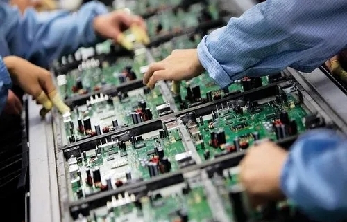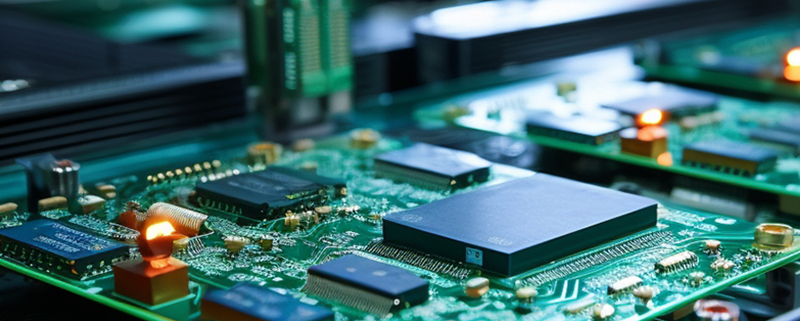
For over two decades, MTI has been dedicated to providing comprehensive OEM/ODM manufacturing services to customers worldwide. With our extensive expertise in PCB assembly, we have established strong collaborative relationships with authorized component distributors. This allows us to source any required components at competitive prices, ensuring cost-effectiveness for our clients.
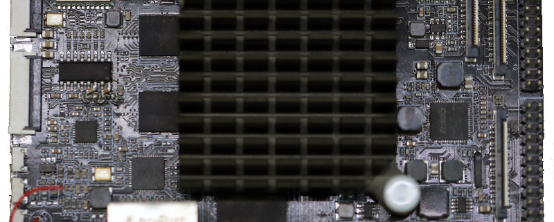
| Product name | 10 layer pcb stack up |
| Keyword | 3080 fe pcb,104 key keyboard pcb |
| Place of Origin | China |
| Board Thickness | 1~3.2mm |
| Applicable Industries | new energy, etc. |
| Service | OEM/ODM manufacturing |
| Certificate | ISO-9001:2015, ISO-14001:2015,ISO-13485:2012.UL/CSA |
| Solder Mask Color | Green |
| Advantage | We keep good quality and competitive price to ensure our customers benefit |
| Sales country | All over the world for example:Australia,India,Syria,Mayotte,Colombia,Poland,Bolivia |
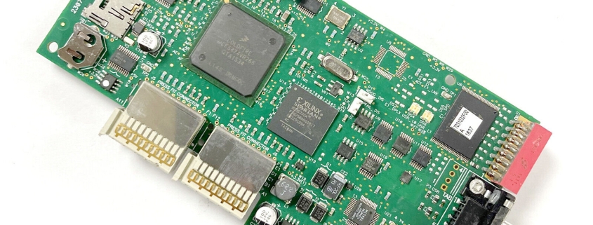
We have rich experience engineer to create a layout using a software platform like Altium Designer. This layout shows you the exact appearance and placement of the components on your board.

Your deliverables are always ahead of schedule and of the highest quality.

One of our Hardware Design Services is small-batch manufacturing, which allows you to test your idea quickly and verify the functionality of the hardware design and PCB board.

FAQs Guide
2.What are the factors to consider when choosing the right PCB material for a specific application?
3.What is thermal management in PCBs and why is it important?
4.Can PCBs have different shapes and sizes?
5.What are the different types of through-hole mounting techniques used in PCBs?
6.What is testability in PCB design and how is it achieved?
1.How does the type of vias used affect the performance of a PCB?
Being one of the top 10 layer pcb stack up manufacturers in China, We attach great importance to this detail.
The type of vias used can affect the performance of a PCB in several ways:
1. Signal Integrity: Vias can act as discontinuities in the signal path, causing reflections and signal degradation. The type of via used can impact the impedance and signal integrity of the PCB. For high-speed signals, it is important to use controlled impedance vias to maintain signal integrity.
2. Electrical Performance: The type of via used can also affect the electrical performance of the PCB. For example, through-hole vias have lower resistance and inductance compared to blind or buried vias, which can affect the power delivery and signal transmission on the PCB.
3. Thermal Performance: Vias can also play a role in the thermal performance of a PCB. Through-hole vias can act as thermal vias, allowing heat to dissipate from one layer to another. Blind and buried vias, on the other hand, can trap heat and affect the overall thermal management of the PCB.
4. Manufacturing Cost: The type of via used can also impact the cost of manufacturing the PCB. Blind and buried vias require more complex and expensive processes, while through-hole vias are relatively simpler and cheaper to manufacture.
5. PCB Size and Density: The type of via used can also affect the size and density of the PCB. Blind and buried vias take up less space on the surface of the PCB, allowing for higher density designs. This can be beneficial for smaller and more compact PCBs.
Overall, the type of vias used can have a significant impact on the performance, cost, and design of a PCB. It is important to carefully consider the type of vias needed for a specific application to ensure optimal performance and functionality of the PCB.
2.What are the factors to consider when choosing the right PCB material for a specific application?
We are centered on customers and always pay attention to customers’ needs for 10 layer pcb stack up products.
1. Electrical properties: The electrical properties of the PCB material, such as dielectric constant, loss tangent, and insulation resistance, should be carefully considered to ensure optimal performance for the specific application.
2. Thermal properties: The thermal conductivity and coefficient of thermal expansion of the PCB material are important factors to consider, especially for applications that require high power or operate in extreme temperatures.
3. Mechanical properties: The mechanical strength, stiffness, and flexibility of the PCB material should be evaluated to ensure it can withstand the physical stresses and strains of the application.
4. Chemical resistance: The PCB material should be resistant to any chemicals or solvents that it may come into contact with during its use.
5. Cost: The cost of the PCB material should be considered, as it can vary significantly depending on the type and quality of the material.
6. Availability: Some PCB materials may be more readily available than others, which can affect production timelines and costs.
7. Manufacturing process: The chosen PCB material should be compatible with the manufacturing process, such as etching, drilling, and plating, to ensure efficient and reliable production.
8. Environmental factors: The application environment, such as humidity, moisture, and exposure to UV light, should be taken into account when selecting a PCB material to ensure it can withstand these conditions.
9. Signal integrity: For high-frequency applications, the PCB material should have low signal loss and good signal integrity to prevent interference and ensure accurate signal transmission.
10. RoHS compliance: If the application requires compliance with environmental regulations, such as the Restriction of Hazardous Substances (RoHS) directive, the PCB material should be chosen accordingly.
3.What is thermal management in PCBs and why is it important?
We have been working hard to improve service quality and meet customer needs.
Thermal management in PCBs (Printed Circuit Boards) refers to the techniques and strategies used to control and dissipate heat generated by electronic components on the board. It is important because excessive heat can damage components, reduce their performance, and even cause the PCB to fail. Proper thermal management is crucial for ensuring the reliability and longevity of electronic devices.
The electronic components on a PCB generate heat due to the flow of electricity through them. This heat can build up and cause the temperature of the PCB to rise, potentially leading to malfunctions or failures. Thermal management techniques are used to dissipate this heat and maintain the temperature of the PCB within safe operating limits.
There are several methods of thermal management in PCBs, including heat sinks, thermal vias, and thermal pads. Heat sinks are metal components attached to hot components on the PCB to absorb and dissipate heat. Thermal vias are small holes drilled into the PCB to allow heat to escape to the other side of the board. Thermal pads are used to transfer heat from components to the PCB and then to the surrounding air.
Proper thermal management is especially important in high-power and high-density PCBs, where heat generation is more significant. It is also crucial in applications where the PCB is exposed to extreme temperatures or harsh environments. Without effective thermal management, the performance and reliability of electronic devices can be compromised, leading to costly repairs or replacements.

4.Can PCBs have different shapes and sizes?
Our company has many years of 10 layer pcb stack up experience and expertise.
Yes, PCBs (printed circuit boards) can have different shapes and sizes depending on the specific design and purpose of the circuit. They can range from small and compact to large and complex, and can be rectangular, circular, or even irregularly shaped. The shape and size of a PCB is determined by the layout of the components and the desired functionality of the circuit.
5.What are the different types of through-hole mounting techniques used in PCBs?
We have flexible production capacity. Whether you are large orders or small orders, you can produce and release goods in a timely manner to meet customer needs.
1. Through-Hole Plating: This is the most common through-hole mounting technique, where the holes in the PCB are plated with a conductive material, usually copper, to create a connection between the layers of the board.
2. Through-Hole Soldering: In this technique, the components are inserted into the plated holes and then soldered to the pads on the opposite side of the board. This provides a strong mechanical connection and good electrical conductivity.
3. Through-Hole Riveting: In this method, the components are inserted into the plated holes and then secured with a rivet or pin. This is commonly used for high-power components or in applications where the board may experience high levels of vibration.
4. Through-Hole Press-Fit: This technique involves inserting the component leads into the plated holes and then pressing them into place using a specialized tool. This provides a strong mechanical connection without the need for soldering.
5. Through-Hole Wave Soldering: In this method, the components are inserted into the plated holes and then passed over a wave of molten solder, which creates a strong solder joint between the component leads and the PCB pads.
6. Through-Hole Reflow Soldering: This technique is similar to wave soldering, but instead of passing over a wave of molten solder, the board is heated in a controlled environment to melt the solder and create a strong joint.
7. Through-Hole Hand Soldering: This is a manual method of soldering where the components are inserted into the plated holes and then soldered by hand using a soldering iron. This is commonly used for small-scale production or for repairs.
8. Through-Hole Pin-in-Paste: This technique involves inserting the component leads into the plated holes and then applying solder paste to the holes before reflow soldering. This provides a strong mechanical connection and good solder joints.
9. Through-Hole Pin-in-Hole: In this method, the component leads are inserted into the plated holes and then bent to form a right angle, creating a secure mechanical connection. This is commonly used for components with large leads, such as electrolytic capacitors.
10. Through-Hole Hand Assembly: This is a manual method of assembly where the components are inserted into the plated holes and then secured with hand tools, such as screws or nuts. This is commonly used for large or heavy components that require additional support.
6.What is testability in PCB design and how is it achieved?
Our 10 layer pcb stack up products undergo strict quality control to ensure customer satisfaction.
Testability in PCB design refers to the ease and accuracy with which a printed circuit board (PCB) can be tested for functionality and performance. It is an important aspect of PCB design as it ensures that any defects or issues with the board can be identified and addressed before it is put into use.
Achieving testability in PCB design involves implementing certain design features and techniques that make it easier to test the board. These include:
1. Design for Test (DFT): This involves designing the PCB with specific test points and access points that allow for easy and accurate testing of different components and circuits.
2. Test Points: These are designated points on the PCB where test probes can be connected to measure voltage, current, and other parameters. Test points should be strategically placed to provide access to critical components and circuits.
3. Test Pads: These are small copper pads on the PCB that are used for attaching test probes. They should be placed close to the corresponding component or circuit for accurate testing.
4. Test Jigs: These are specialized tools used for testing PCBs. They can be custom-made for a specific PCB design and can greatly improve the accuracy and efficiency of testing.
5. Design for Manufacturability (DFM): This involves designing the PCB with manufacturing and testing in mind. This includes using standard components, avoiding complex layouts, and minimizing the number of layers to make testing easier.
6. Design for Debug (DFD): This involves designing the PCB with features that make it easier to identify and troubleshoot any issues that may arise during testing.
Overall, achieving testability in PCB design requires careful planning and consideration of the testing process. By implementing DFT, using test points and pads, and designing for manufacturability and debug, designers can ensure that their PCBs are easily testable and can be quickly and accurately diagnosed for any potential issues.

Tags:circuit card assembly vs pcb,printed circuit board assembly suppliers